

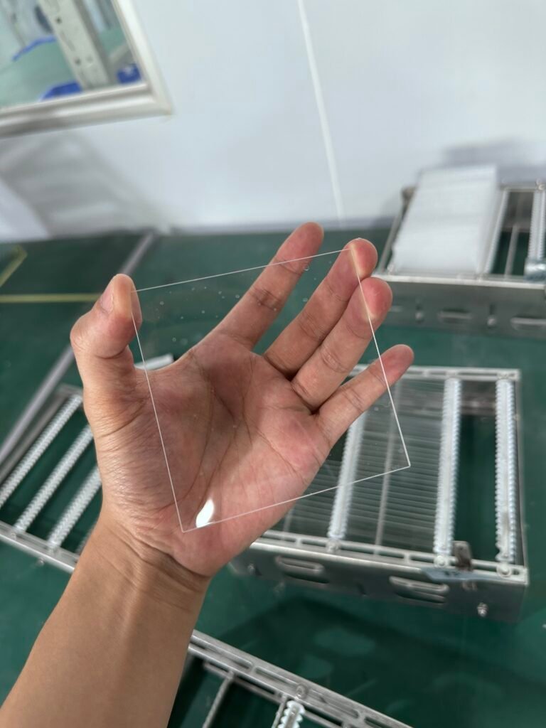
Double-Sided Polished Glass: TTV, Surface Roughness, Flatness & Applications
Distinguish TTV, flatness, parallelism, bow, warp, roughness and scratch-dig when specifying polished windows, wafers and optical substrates.
Engineering guides covering glass materials, surface finishing, precision processing, dimensional tolerances, inspection methods, and application-specific material selection.
Distinguish TTV, flatness, parallelism, bow, warp, roughness and scratch-dig when specifying polished windows, wafers and optical substrates.
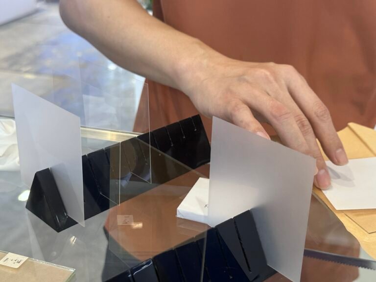
Compare three glass surface finishes by optical function, downstream compatibility and inspection requirements, then follow the relevant in-depth guide.
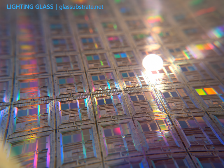
A technical guide to semiconductor wafer double-side polishing (DSP): its place in wafer manufacturing, mechanical and chemical action, TTV, bow, warp, surface quality and its value for MEMS, SOI and bonding.

See how glass material, thickness, TTV, flatness, edges and handling affect optical-module assembly. A practical guide to drawings and inspection.
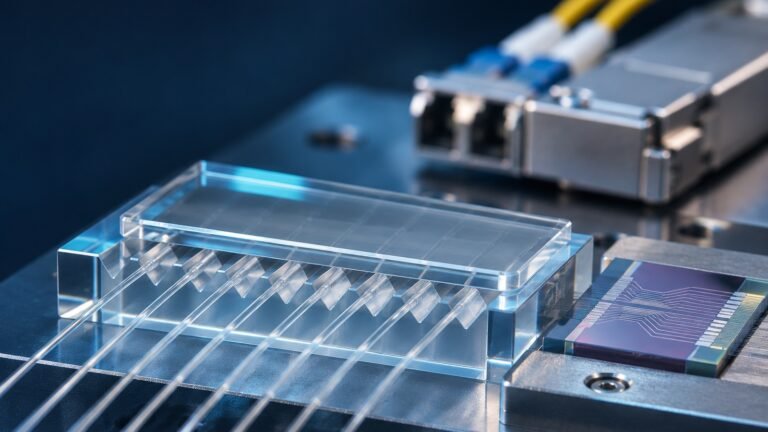
How V-groove substrates and glass lids position fiber arrays for CPO and photonic chips. Learn coupling-loss assumptions, tolerance stacks, inspection and RFQ requirements.

Explore common glass families used in optics, from imaging glass and fused silica to filters and electronic substrates. Learn which specifications to verify before selecting a grade.
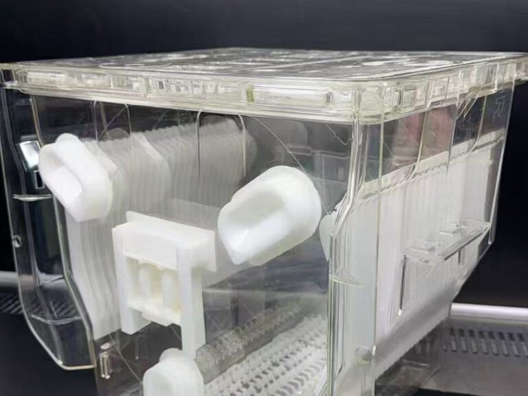
Compare BOROFLOAT 33 with TGV substrate requirements: thermal expansion, via-process compatibility, thickness, surface quality and a practical procurement checklist.
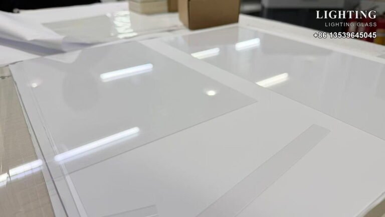
Check SCHOTT BOROFLOAT® 33 thermal and optical data, 20 standard thicknesses, sheet sizes and practical material-verification steps before requesting a quote.