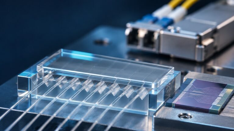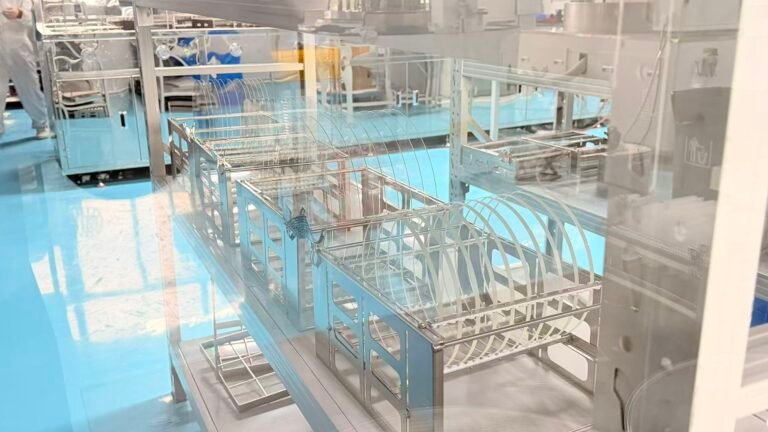


In semiconductor manufacturing, one process is fundamental yet directly affects downstream yield and the limits of device performance: DSP (Double Side Polishing).
If chip manufacturing were compared to constructing a skyscraper, the wafer would be more than its “floor.” It would be the reference plane for the entire building.
- That reference plane must be pure as well as flat;
- it must be flat, with both sides under control;
- and it must do more than “look like a mirror.” Thickness, parallelism, bow and warp, surface roughness and edge profile must all fall within strict industrial process windows.
This is why DSP has never been as simple as “making a silicon wafer shiny.” It is high-precision surface and geometry engineering shaped by the requirements of subsequent lithography, bonding, double-sided processing, MEMS (Micro-Electro-Mechanical Systems), RF (radio-frequency) devices and power devices.
Often, the deciding factor for a wafer fab, a device line or a packaging scheme is not whether a process can be carried out, but whether its process window is wide enough.
The significance of DSP lies in turning a wafer from a “usable material” into a “substrate suitable for high-precision manufacturing.”
In advanced manufacturing, this step is the foundation, not a supporting act.

01 | DSP: A Wafer with Both Sides Inside the Precision Manufacturing Window
As its name suggests, DSP (Double Side Polishing) means that both the front and back surfaces of a wafer receive precision polishing.
Compared with SSP (Single Side Polished), the main difference is not simply that “one more side is polished.” Both sides must satisfy tighter surface and geometric quality requirements.
SEMI (Semiconductor Equipment and Materials International) states in its specification for polished single-crystal silicon wafers that a prime wafer has at least one chem-mechanically polished surface. This also means that not every wafer must undergo DSP.
DSP is more relevant to applications that are particularly sensitive to the condition of both surfaces, parallelism between the sides, subsequent double-sided processes and bonding consistency.
This is why industry discussions of DSP focus on a “functional mirror surface,” rather than a mirror-like appearance.
For example, Okmetic describes its DSP wafers as a platform for surface MEMS, cap wafers, RF devices and power devices. It also emphasizes thickness uniformity, orientation accuracy, suitability for double-sided lithography, and the bonding strength and hermetic sealing value of MEMS caps.
In other words, DSP is not about appearance. It helps the subsequent processes become feasible, manageable and stable.
Put more simply: SSP resembles a “substrate processable on one side,” while DSP resembles a “precision substrate that can be engineered on both sides.”
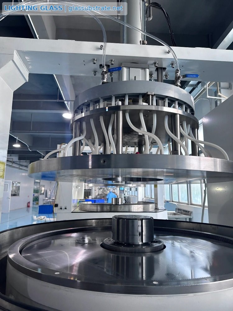
02 | Where DSP Fits in Wafer Manufacturing: Not the Start, but It Sets the Starting Conditions
Silicon wafer manufacturing can generally be divided into two broad stages: growing a single-crystal silicon ingot, and then processing that ingot into wafers ready for chip manufacturing.

SUMCO describes a typical wafer-forming sequence. After the single-crystal ingot is sliced, lapping brings thickness and parallelism into the target range. Etching then removes mechanical damage from preceding operations. Polishing follows, using mechano-chemical action, typically with colloidal silica, to produce a highly flat, mirror-finished wafer surface.
Siltronic likewise describes a polished wafer as a product that acquires a “virtually perfect surface” through CMP (Chemical Mechanical Polishing).
DSP, therefore, is not an isolated cosmetic operation. It is one of the key finishing stages toward the end of wafer manufacturing.
The earlier slicing, lapping and etching steps address the transition “from ingot to wafer”; polishing addresses the transition “from wafer to manufacturing substrate.”
DSP matters because it turns a silicon slice, understood merely as a material, into an industrial reference surface on which lithography, bonding, double-sided patterning, film growth and microstructuring can rely.
In semiconductor processing, the most expensive mistakes often do not arise because “too little was done at this step,” but because the earlier reference surface was not good enough.
DSP helps compress many potential deviations before they reach the dozens or even hundreds of processes that follow.
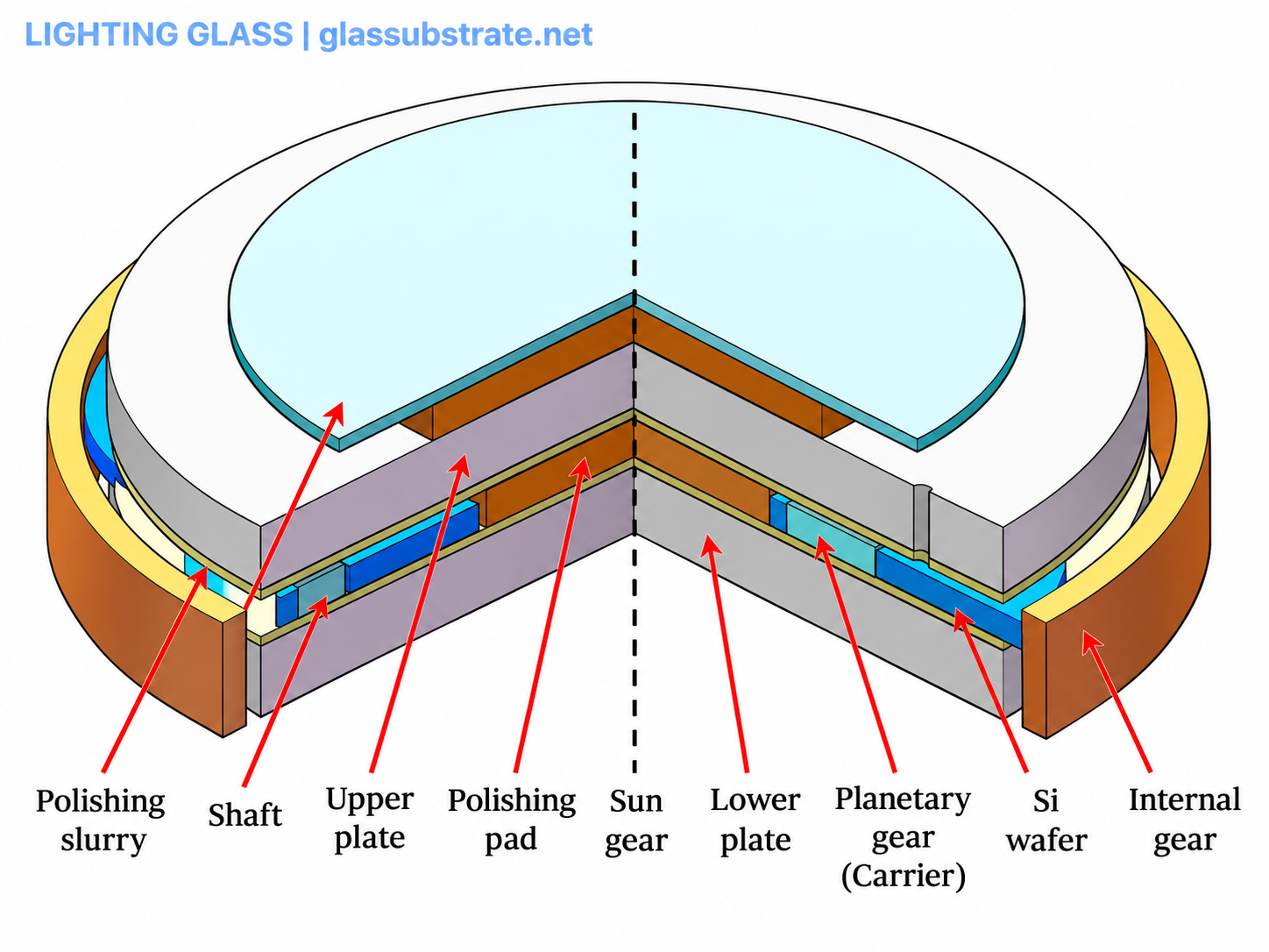
03 | How DSP Polishes a Wafer: A Precise Balance of Mechanical and Chemical Action
The point of DSP in semiconductor manufacturing is not aggressive material removal. It is to remove material in a controlled way without introducing new damage, while bringing the surfaces, parallelism, edge profile and uniformity into the required condition.
As described by SUMCO and Siltronic, modern wafer polishing involves both mechanical action and chemical reactions.
The mechanical component removes surface material and improves form; the chemical component modifies the surface and helps achieve less damage and higher surface quality.
Equipment suppliers also identify removal-rate uniformity and edge-profile accuracy as key metrics.
In its description of a 300 mm final polisher, Okamoto highlights edge-profile accuracy and removal-rate uniformity. This shows that the real challenge is not whether polishing can be done, but whether results are consistent across the wafer, around its edge, on both sides and from batch to batch.
Why is this step difficult?
Because a wafer is not an ordinary metal plate.
It is thin, brittle and large, while the forces, fluid conditions, abrasive distribution and thermal effects at its edge differ from those at its center.
- Polish too quickly, and the surface may look bright while subsurface damage, microscratches, abnormal edge removal and residual stress emerge;
- polish too slowly, and productivity may be too low, cost too high and the process window too narrow.
For wafers that will be bonded, surface roughness and particle control are more than a simple exercise in making the surface “as good as possible.” They directly affect whether the wafers can achieve intimate contact.
EV Group makes this clear in its discussion of direct bonding:
Excessive surface roughness prevents sufficient contact and leads to low bond strength or no bond at all. Particle contamination causes voids, while a mismatch in coefficients of thermal expansion can cause wafer bow and cracks.
Thus, what DSP really establishes is not merely surface brightness, but consistency for subsequent manufacturing.
04 | How to Evaluate DSP: Look Beyond Shine to the Critical Metrics
In semiconductor manufacturing, DSP quality is usually assessed through geometric and surface metrology, not by eye.
SEMI specifications and guides repeatedly identify thickness, TTV (Total Thickness Variation), bow, warp and flatness as critical parameters for later manufacturing steps.
SEMI also notes that controlling these parameters is fundamental and necessary for many semiconductor processes.
TTV, bow and warp are the three concepts most easily confused here.
- TTV describes how uniform the wafer's thickness is;
- bow describes the wafer's overall bending relative to a reference plane;
- warp describes a more comprehensive overall deformation.
In simple terms, even when a wafer has the correct average thickness, a nonuniform thickness distribution can create a TTV problem. Even with good TTV, a wafer that arches like a dish can still have bow and warp that affect subsequent processes.
In advanced manufacturing, these are not merely numbers on a supplier's report. They are process variables that propagate into lithographic alignment, film stress, stacking errors and the stability of equipment clamping.
KLA points out that, in advanced memory, DRAM (Dynamic Random Access Memory) and logic manufacturing, wafer shape, stress and distortion directly affect overlay and subsequent process control.
Its systems also measure shape, thickness, front- and back-side nanotopography, and ERO (Edge Roll Off).
That is why excellent DSP requires more than a mirror-like surface: uniform thickness across the wafer, parallel sides, controlled edge transitions, low surface roughness, few particles and small local height variations all matter.
For example, Okmetic lists typical specifications for its 150–200 mm DSP products that include TTV below 1 µm and orientation accuracy up to ±0.2°. These figures illustrate the point:
Competition in DSP is not about whether a wafer was processed, but how tightly its errors can be controlled.
Of course, these are examples of one supplier's product specifications. They do not apply uniformly to every diameter, material or application.

05 | Where DSP Matters Most: Why the Higher Cost Can Be Worth It
Not every chip process must begin with DSP. But DSP becomes increasingly important where double-sided processing, direct bonding, MEMS caps, SOI (Silicon On Insulator), precision micromechanical structures, and certain RF and power devices are involved.
Okmetic identifies surface MEMS, capping wafers, RF devices and power devices as applications for its DSP wafers.
It also emphasizes their suitability for double-sided lithography, MEMS cap bonding, and anisotropic etching with KOH (Potassium Hydroxide) or TMAH (Tetramethylammonium Hydroxide).
The logic is clear: once device manufacturing requires the back side to participate in processing, DSP ceases to be an optional advantage and becomes a foundation.
The next step in complexity involves wafer bonding and SOI.
Soitec explains that Smart Cut™ combines light-ion implantation and molecular bonding to transfer an ultrathin single-crystal layer from one substrate to another. In schemes such as Smart Stacking™, direct bonding is followed by mechano-chemical thinning.
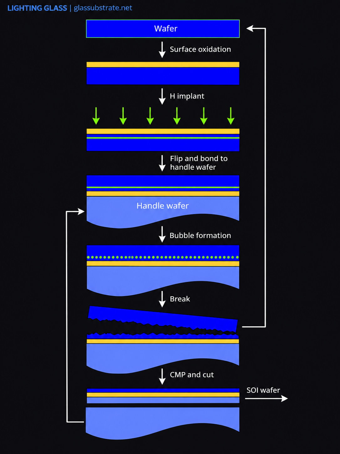
The demands on surface condition, thickness uniformity and interface cleanliness are extremely high. If the surface is rough, particles are excessive or TTV is too large, voids, concentrated stress or even cracks can arise at the bonding interface.
Discussions of wafer bonding by EV Group and the Journal of Semiconductors likewise identify surface roughness, cleanliness, thermal-expansion mismatch and TTV as factors affecting bonding success and interface quality.
Why, then, does DSP cost more?
Because it performs high-precision surface engineering on both sides of a wafer. The process window is narrower, metrology more complex, cleaning more stringent, yield control more difficult, edge behavior more troublesome and batch-to-batch consistency more demanding.
Why can it still be worth the cost?
Because the result is not a “higher-grade appearance.” It is double-sided process capability, more stable bonding, more reliable packaging, a better geometric reference and a wider window for subsequent manufacturing.
DSP can be understood as an “upfront investment”: it addresses difficulties at the substrate stage before errors and costs multiply in downstream processes.
For advanced semiconductors, the most expensive thing is not any single process, but using an inadequate substrate for many expensive processes.
From this perspective, DSP is a center of risk control rather than merely a cost center.
06 | Conclusion
Looking back at DSP, we see a familiar truth of semiconductor manufacturing: the more advanced an industry becomes, the more it relies on fundamental processes that may appear less spectacular.
The value of a truly excellent DSP wafer is not simply that “it has been polished.” It lies in giving engineers, in advance, the qualities needed by subsequent manufacturing: flatness, stability, cleanliness and precision.
For double-sided lithography, MEMS, SOI, direct bonding, RF and some power devices, DSP is not a dispensable premium option. It is the invisible mirror surface that helps determine both the manufacturing baseline and the ceiling of performance.
As the industry moves toward smaller line widths, more complex structures and greater integration, people see more powerful chips. The wafer beneath them, sufficiently well controlled on both sides, is where many of those stories actually begin.