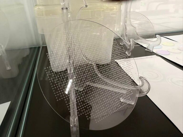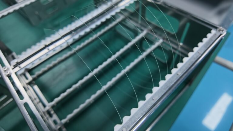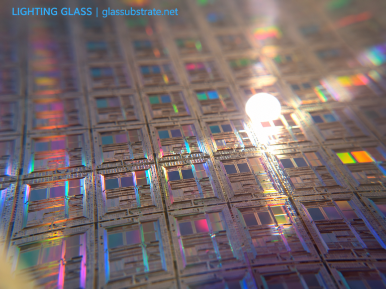


Semiconductor glass substrates can provide optical access, electrical isolation, structural support or a process interface. MEMS covers, glass wafers, temporary carriers and TGV substrates impose different requirements. Selection needs the material and the downstream manufacturing sequence together, rather than a comparison of transparency or price alone.
Choose material for the actual interface
Silicon-to-glass anodic bonding depends on glass composition and the bonding mechanism as well as thermal compatibility. A thin-film substrate may emphasize composition, surface state and thermal stability. An optical sensor cover requires grade- and thickness-specific transmission and surface quality. A temporary carrier additionally needs compatibility with the adhesive, thermal cycle and debonding process.
| Application | Material direction to evaluate | Questions that remain |
|---|---|---|
| MEMS anodic-bonded cover | A borosilicate grade qualified for the intended bonding process | Actual bonding recipe, chemistry, surface condition and thermal mismatch. |
| Thin-film or electronic substrate | Appropriate alkali-free or other process-compatible glass. | Composition, deposition compatibility and heat-treatment stability. |
| UV optical component | Specified fused-silica grade. | Transmission at the operating wavelength, thickness and contamination. |
| Temporary carrier | Glass selected for the specific carrier process. | Mechanical handling, shape, adhesive and debonding compatibility. |
Borosilicate glass may be considered for MEMS covers, optical sensing and wafer-level packaging when its composition, thermal expansion, surface condition and bonding process have been qualified together. Do not transfer one manufacturer’s sheet specifications to another grade or to the finished part.
Specify thickness and wafer geometry separately
Nominal thickness, thickness tolerance and TTV are separate requirements. Bow, warp, flatness and parallelism also require distinct definitions. Specify mapping, edge exclusion, support and uncertainty. Manufacturer values for a designated starting wafer must not become guarantees for every cut or drilled component.
Thin substrates can deform during handling and measurement. Identify free-state and constrained requirements according to the downstream process. A useful inspection plan records how the sample is supported and which surface or median-surface quantity is reported. See the detailed double-sided polishing guide.
Polishing is only one part of bonding readiness
A double-polished description does not establish bonding suitability. Surface texture, particles, residue and chemistry can all affect contact. Qualify the final cleaning, storage and bonding sequence with representative components. Define critical areas rather than applying a generic “semiconductor grade” label.
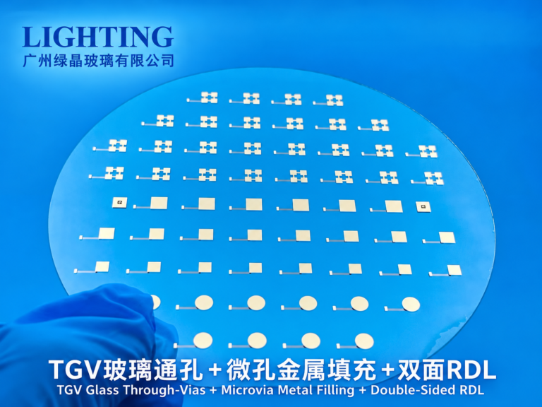
A through-glass opening is not a finished conductive via
TGV procurement should specify hole openings, taper, position, wall condition and rim defects. Hole metallization, electrical continuity and reliability are additional processes with separate responsibilities. Hole quality can affect later coating and metallization, while drilling can disturb a previously accepted polished surface.
The laser drilling guide explains why a nominal diameter alone is incomplete. Evaluate the material, thickness, hole array and downstream sequence together.
Match standards to their scope
Do not label silicon-wafer metrology as a universal glass-wafer specification. SEMI MF1530-0707, reapproved 0824, has a silicon-wafer scope. A transparent-glass measurement method needs validation for its sensing principle and sample conditions. SEMI 3D2 concerns a particular glass-carrier use; verify the applicable current document before incorporating it into a contract.
Compare quotations on the same acceptance basis
Supply a drawing revision, material grade, dimensions, thickness, quantity and process sequence. Identify functional surfaces, edge contour, holes and permitted substitutions. Ask for the same inspection conditions and delivered cleaning state when comparing suppliers. Excessively strict nonfunctional limits add cost; omitted functional requirements can cause downstream rejection.
Preparing a substrate RFQ
Include TTV and shape requirements where needed, with their test conditions. Add bonding, coating, metallization and thermal-cycle information, then specify relevant surface quality, cleaning and packaging. Request sample qualification for the actual process rather than assuming a catalogue material value is a final-part guarantee.
Borosilicate glass processing · BOROFLOAT 33 material · Acceptance planning
Technical references
- .
- SCHOTT — BOROFLOAT technical details.
- SEMI MF1530 — metrology scope.
Product data and application directions require project-specific verification. This guide makes no claim of company cleanroom certification, metallization capability or guaranteed substrate limits.