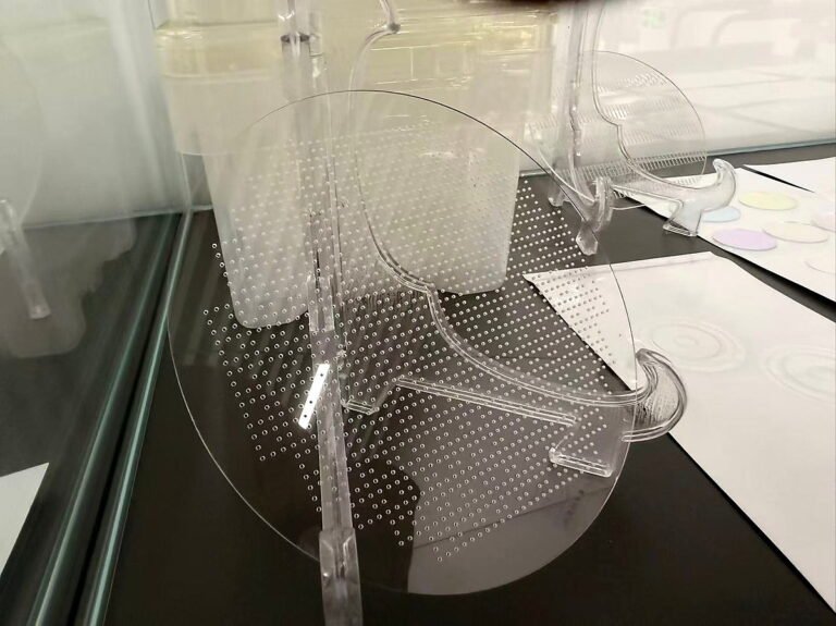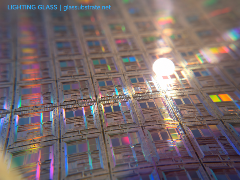


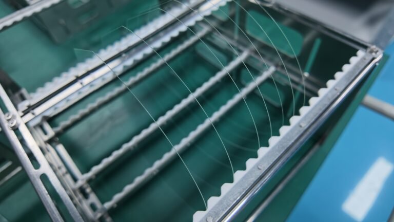
A glass wafer is a circular glass substrate designed for wafer-level equipment or processing. Depending on its material and subsequent fabrication, it can serve as an optical substrate, a MEMS cap, a temporary carrier, or part of an interconnect structure with through-glass vias (TGVs). The term “glass wafer” describes a shape and process interface, not a particular glass composition. An optical glass wafer also has to meet the optical requirements of its specific design. Optical and packaging applications therefore cannot share one universal specification for wavelength range, thermal expansion, thickness, surface condition or cleanliness.
1. What does the inch designation mean?
In wafer processing, 150, 200 and 300 mm diameters are commonly called 6, 8 and 12 inches. These are industry size names: 300 mm is not the exact conversion of 12 inches, which is 304.8 mm. Specify the actual glass wafer diameter in millimetres, together with its tolerance, drawing and applicable acceptance criteria. Do not assume that a silicon-wafer standard automatically defines a glass wafer.
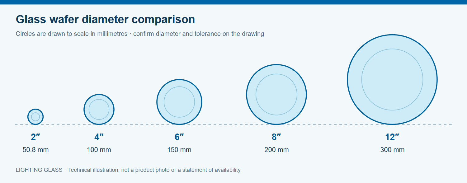
Figure 1. Circles are drawn to scale using the nominal millimetre diameters. This is a technical illustration, not a product photograph.
| Common size name | Common matching nominal diameter | Exact inch conversion | Clarify when purchasing |
|---|---|---|---|
| 2 inch | 50.8 mm | 50.8 mm | Actual diameter and tolerance |
| 4 inch | 100 mm | 101.6 mm | Whether 100 or 101.6 mm is required |
| 6 inch | 150 mm | 152.4 mm | Nominal diameter and orientation feature |
| 8 inch | 200 mm | 203.2 mm | Diameter, notch and carrier interface |
| 12 inch | 300 mm | 304.8 mm | Diameter, notch and equipment interface |
The 4–12-inch entries reflect common wafer-equipment terminology, not a mandatory size series for every glass product. An order should state nominal diameter and tolerance in millimetres, edge profile, and any orientation flat or notch. A larger diameter does not produce a proportional increase in usable parts: the area of a 300 mm circle is 2.25 times that of a 200 mm circle, while edge exclusion, layout, defects, yield and carriers determine the actual output.
2. What does a glass wafer do?
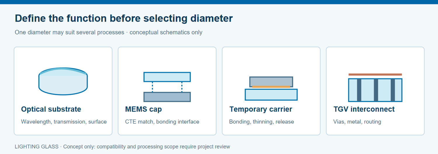
Figure 2. Four possible functions. Diameter alone does not define the material, structure or process.
Optical substrate. A glass wafer may be processed into waveguides, coated optics or micro-optical components. A high-index wafer for an augmented-reality waveguide is one example. Refractive index, homogeneity, birefringence, transmission, thickness uniformity and surface quality all matter. Confirm the exact grade and available diameter from the relevant material documentation.
MEMS cap and sensor package. Glass may form a viewing window, cavity cap or bonding interface. For anodic bonding to silicon, verify the selected grade's suitability, thermal expansion over the relevant temperature range and surface condition. “Borosilicate” alone is not proof that any particular grade can be bonded directly.
Temporary carrier. A glass carrier supports a device wafer during thinning, wafer-level packaging and release. The bonding and debonding method, laser wavelength where relevant, thermal history and flatness must be considered together.
TGV interconnect substrate. Through-glass vias, metallization and redistribution layers may form part of an interposer or wafer-level package. Via diameter, profile and pitch constrain the usable thickness. A plain glass wafer has not necessarily undergone via formation or metallization.
3. How should 2, 4, 6, 8 and 12 inches be evaluated?
The following are starting points for specification discussions, not exclusive applications or a claim that every material and process is available at every diameter. Suitability depends on material, equipment interface and process qualification.
| Size class | Possible project direction | Check first |
|---|---|---|
| 2 inch / about 50.8 mm | Small-scale process validation and optical or microsystem samples | Actual diameter, tooling and minimum order quantity |
| 4 inch / 100 mm | MEMS caps, sensors and bonding development | Grade, bondability, flat or notch |
| 6 inch / 150 mm | Optical wafers, MEMS, sensors and some TGV concepts | Thickness, TTV, surface and via geometry |
| 8 inch / 200 mm | Wafer-level package carriers, optical wafers and TGV concepts | Carriers, warp, cleanliness and downstream equipment |
| 12 inch / 300 mm | Large carriers, optical wafers and some advanced-package interconnect concepts | 300 mm interface, deformation, edge and inspection area |
Products at these diameters exist, but size ranges vary by material family and manufacturing route. Specifications from different manufacturers must not be combined into a single claimed grade or LIGHTING GLASS capability.
4. Select the material for the application, not the diameter alone
| Material family | Typical consideration | Confirm for the chosen grade |
|---|---|---|
| Optical glass | Waveguides, filters and other optical wafers | Wavelength range, index, dispersion, homogeneity, stress birefringence and transmission |
| Fused quartz glass or synthetic fused silica | Projects involving UV transmission, thermal stability or purity | Feedstock and manufacturing route, grade, wavelength, sample thickness, OH and metal impurities |
| Specified borosilicate grade | MEMS caps, windows and some glass-to-silicon bonding | Expansion throughout the process temperature range, bonding process, thickness and starting surface |
| Alkali-free or low-alkali technical glass | Projects sensitive to ion migration or requiring stable package structures | Composition, dielectric properties, TGV compatibility and metallization |
These categories overlap: fused silica can also be an optical substrate. Crystalline quartz wafers are crystalline material and should not be confused with amorphous fused-quartz glass wafers. A property of one grade cannot be assigned to its entire material family. Thickness availability can also vary at the same diameter; specify material, diameter, thickness and tolerances separately.
5. What belongs on the drawing and inspection plan?
| Item | Why it matters |
|---|---|
| Diameter and orientation | State nominal diameter and tolerance in mm, flat or notch, edge profile and exclusion zone. “8 inch” alone does not define an equipment-ready wafer. |
| Thickness and TTV | Thickness affects handling and downstream processes. Total thickness variation is the difference between maximum and minimum thickness in a defined measurement area; agree on the scan or sampling region. |
| Bow and warp | These describe wafer shape and are not the same as TTV. Specify free or supported measurement state, method and usable area. |
| Surface quality | Identify the required side or sides, roughness metric and method, scratch/dig or defect limits, illumination and inspection zone. |
| Optical requirements | State wavelength, grade and conditions for transmission or reflection. For a spectrum, specify sample thickness, surface condition and coating status. |
| Features and cleanliness | Define vias, blind holes, metallization or coatings in separate drawings and acceptance criteria. Include cleaning, particle limits, packaging and transport. |
There is no useful universal transmission spectrum for “glass wafers.” Grade, thickness, surface and coating change the curve. Request a grade-specific manufacturer document or measurement under the required conditions instead of reusing another glass's spectrum.
6. Processing route: from starting sheet to delivery
Depending on the intended function, work may include material verification, circular shaping, edge finishing, grinding or double-side polishing, cleaning, feature formation, coating, pre-bond inspection and packaging in dedicated carriers. Not every wafer requires the same sequence. Some thin drawn-glass wafers retain their original surface; high-precision optical wafers may need further polishing and thickness-uniformity control. A TGV design also requires an assessment of hole geometry and subsequent metallization.
For large, thin wafers, handling and shape control must be assessed with thickness and support method. Gravity and support can affect form measurements, so inspection reports should state the measurement condition.
Frequently asked questions
Is a 12-inch glass wafer always 304.8 mm? No. In wafer manufacturing, “12 inch” usually denotes the 300 mm class; 304.8 mm is the exact mathematical conversion of a length. Put the required diameter and tolerance in millimetres on the purchase drawing.
Can any transparent glass be used for anodic bonding or TGV? No. These processes place different demands on composition, thermal expansion, surface, electrical properties and structural compatibility. Qualify the selected grade and process.
May allowable TTV simply increase in proportion to wafer diameter? No. The acceptable value depends on the downstream process, active device area, measurement method and project acceptance criteria.
What should I send for a quotation or fabrication review? Provide the grade or candidate materials, application, diameter and tolerance in mm, thickness, flat or notch, surface and TTV requirements, optical wavelength, feature drawing, quantity and downstream process. Mark undecided parameters as “to be evaluated.”
Review your glass wafer drawing
For a project involving glass-wafer cutting, edge finishing, grinding, polishing, hole formation or subsequent assembly, contact us and upload your drawing with the known acceptance criteria. Feasible processing scope, material source and delivery specifications are confirmed after project review.