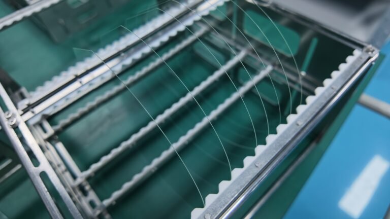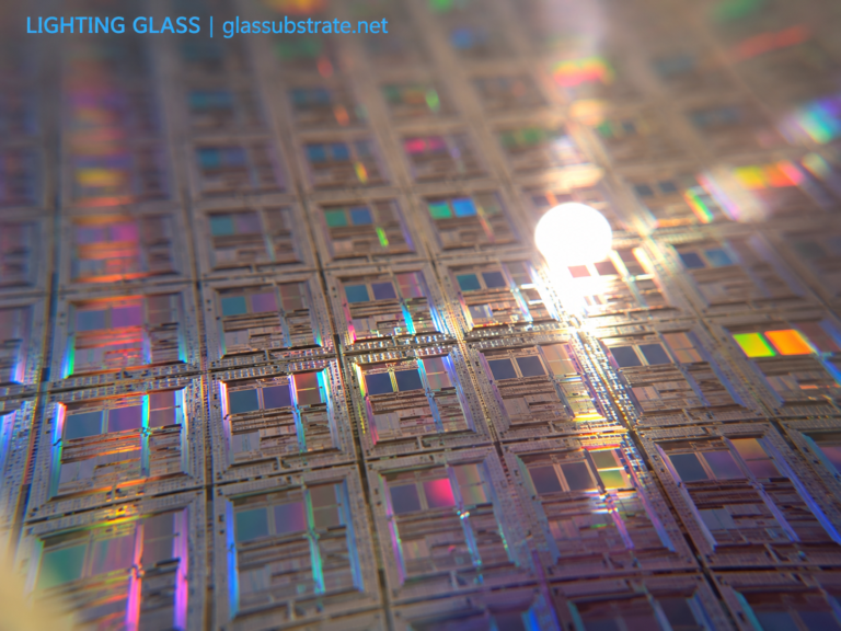

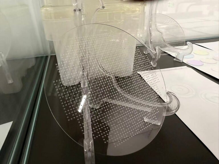
A glass wafer is a circular glass substrate made to work with wafer-level equipment or processes. Depending on its grade and downstream steps, it can serve as a temporary carrier, optical substrate, package cap or insulating base. With suitable via formation, metallization and redistribution layers, it can also support electrical interconnects. “Glass wafer” describes a form and process interface, not a single glass composition. Select the material from the device function, thermal and chemical history, equipment interface and inspection plan.
How is a glass wafer different from a silicon wafer?
A conventional silicon wafer is a single-crystal semiconductor with crystallographic orientation. Most glass wafers are amorphous and electrically insulating, with transmission in a grade-dependent wavelength range. A glass substrate can still become part of an electrical circuit after vias and conductive layers are fabricated. Thermal expansion, dielectric properties and optical transmission must be compared using specific grades and test conditions. Sapphire is crystalline aluminium oxide, not glass; glass-ceramics with crystalline phases must also be distinguished from ordinary amorphous glass.
Six applications and the requirements behind them
Temporary carrier. A device wafer may be bonded to a rigid glass carrier during thinning or transfer. Verify flatness, thermal history, bonding and debonding chemistry. Laser debonding also requires transmission at the actual laser wavelength and carrier thickness.
Fan-out packaging carrier. A reconstructed wafer or package may use a glass carrier for support and a stable processing surface. Carrier design and reuse must be qualified for the chosen process.
TGV interposer. Through-glass vias can provide vertical interconnects after metallization and redistribution. A drilled hole by itself is not a conductive via. See our TGV hole geometry and inspection guide.
MEMS cap wafer. Glass can form an observation window, cavity cap or bonding interface. Package hermeticity depends on the joint and complete assembly, not on the glass alone. For bonding considerations, read the glass wafer bonding guide.
Microfluidic substrate. Channels and chambers formed in glass can support optical observation and chemical analysis. Channel geometry, surface chemistry, sealing and cleaning are part of the design.
Optical waveguide substrate. Some integrated-optics and display waveguides use selected optical glass grades. Refractive index, homogeneity, birefringence, transmission, thickness uniformity and surface quality matter. Such a substrate is a specialized optical application, not a universal semiconductor glass wafer.
Which glass families are considered?
| Material family | Possible role | Verify for the selected grade |
|---|---|---|
| Fused silica or synthetic fused silica | Projects requiring thermal stability, purity or transmission at a specified wavelength | Grade, wavelength, thickness, impurities and manufacturer data |
| Borosilicate glass | Carriers, windows and some MEMS caps | Grade, expansion over the process temperature range, bonding compatibility |
| Low-alkali or alkali-free technical glass | Electronic processes sensitive to mobile-ion contamination | Composition, dielectric behaviour and process compatibility |
| Specified optical glass | Optical windows, waveguides or polished substrates | Index, dispersion, homogeneity, stress birefringence and wavelength range |
“Alkali-free” does not mean that every trace impurity is absolutely zero. Conversely, a process such as anodic bonding may have particular ion-mobility requirements. Do not extend one grade's data to an entire glass family or describe raw-material data as measurements of a finished part.
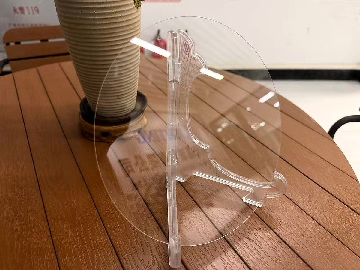
Diameter, thickness and usable area
Nominal 100, 150, 200 and 300 mm wafers are often called 4-, 6-, 8- and 12-inch classes. These are industry labels: exactly 12 inches equals 304.8 mm, not 300 mm. Purchase drawings should specify diameter and tolerance in millimetres, flat or notch, edge profile and carrier interface. Our separate 2–12 inch glass wafer selection guide covers size classes in detail.
| Common class | Nominal diameter | Geometric circle area |
|---|---|---|
| 4 inch | 100 mm | 78.54 cm² |
| 6 inch | 150 mm | 176.71 cm² |
| 8 inch | 200 mm | 314.16 cm² |
| 12 inch | 300 mm | 706.86 cm² |
These values use A = π(d/2)² and describe geometric area only. Edge exclusion, dicing streets, layout and yield reduce usable area. For the same material and geometry, plate bending stiffness scales approximately with thickness cubed; thinner wafers are more flexible. Residual processing stress, films, bonding and temperature can also contribute to deformation.
TTV, bow, warp and flatness are different specifications
| Metric | Meaning | Specify with the limit |
|---|---|---|
| TTV | Maximum thickness minus minimum thickness in the defined area. A range from 0.498 to 0.502 mm gives 4 μm TTV. | Scan area, edge exclusion, sampling and instrument |
| Bow | Centre displacement of the wafer median surface relative to a defined reference plane. | Reference, support state, sign and method |
| Warp | Range of positive and negative median-surface departures from a reference plane; captures more complex shape. | Free or supported state, working area and algorithm |
| Flatness | Departure of a specified surface from a defined reference over a stated area; more specific global or local metrics may be used. | Surface, area, fitted reference and exact metric |
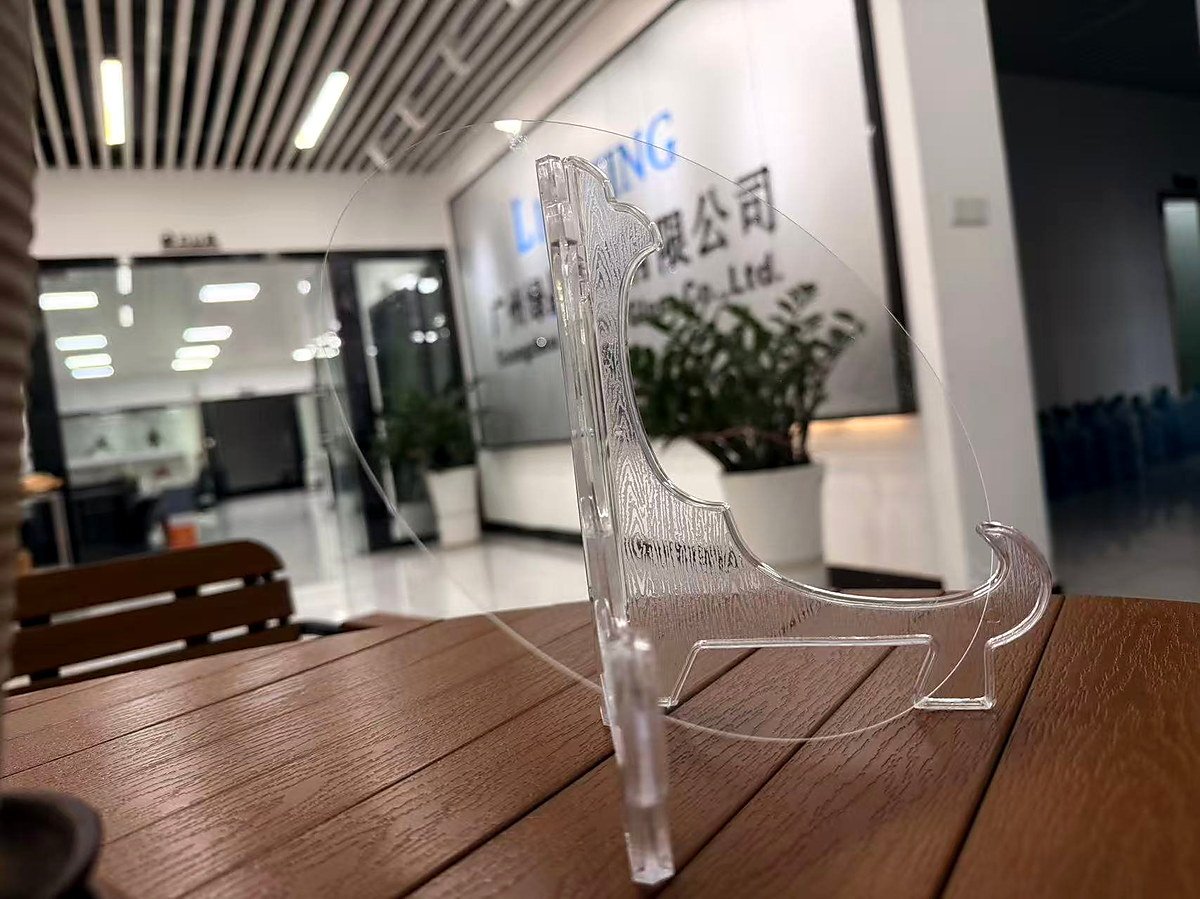
Low TTV does not imply low warp. Nearly parallel faces can still bend together. Gravity and the support arrangement can affect measurements of a low-stiffness wafer; buyer and supplier should use the same definitions and acceptance conditions. Relevant industry metrology guidance includes SEMI 3D4 for bonded wafer stacks and SEMI 3D12 for low-stiffness wafer shape; their scopes should be checked before applying a procedure to a particular glass wafer.
When does the Stoney equation help?
For a film much thinner than an elastic substrate, measured curvature before and after coating can under suitable assumptions estimate average biaxial film stress:
σf = Ests2 / [6(1−νs)tf] × (1/R − 1/R0)
Here Es and νs are substrate elastic modulus and Poisson ratio, ts and tf are substrate and film thicknesses, and R0 and R are curvature radii before and after coating. The curvature sign follows the chosen measurement convention. Ordinary warp values cannot simply be inserted as curvature. Thick or multiple films, non-uniform stress and large deformations require a more suitable model.
What else must be inspected on a TGV wafer?
A via drawing should state diameter, pitch, aspect ratio, entrance and exit dimensions, taper, position, chipping and microcrack criteria, plus separate metallization and electrical acceptance requirements. Photographs can show a hole pattern, but through-hole status, sidewalls and connectivity require their own tests.
Surface requirements may include Ra or Rq with instrument, measurement area and filtering stated. Scratches, digs, particles, edge damage, ions and organic residues can affect coating, bonding, optical performance or packaging. “Clean surface” is not an acceptance criterion without defined contaminants, methods and limits.
Nine items to send with a glass wafer drawing
- Glass grade or candidate materials, working wavelength, temperature and downstream process.
- Diameter and tolerance, thickness, flat or notch, and edge profile.
- TTV limit with scan area and measurement method.
- Bow, warp and flatness limits with support and reference conditions.
- One- or two-sided surface finish, Ra/Rq and scratch–dig criteria.
- Via drawing and any metallization, coating or bonding requirements.
- Cleanliness, packaging and transport requirements.
- Prototype or production quantity, inspection report and traceability needs.
- Any unresolved parameter clearly marked for joint review.
LIGHTING GLASS can review material selection and precision fabrication against your drawing. Send your glass wafer drawing for review with dimensions, quantity and critical acceptance conditions. Feasible scope and delivery specifications are confirmed after project evaluation.