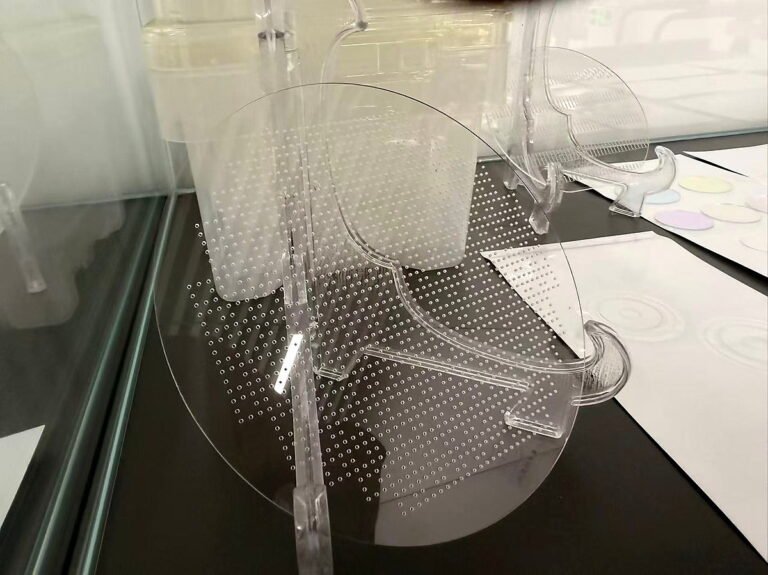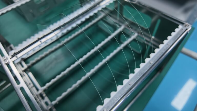


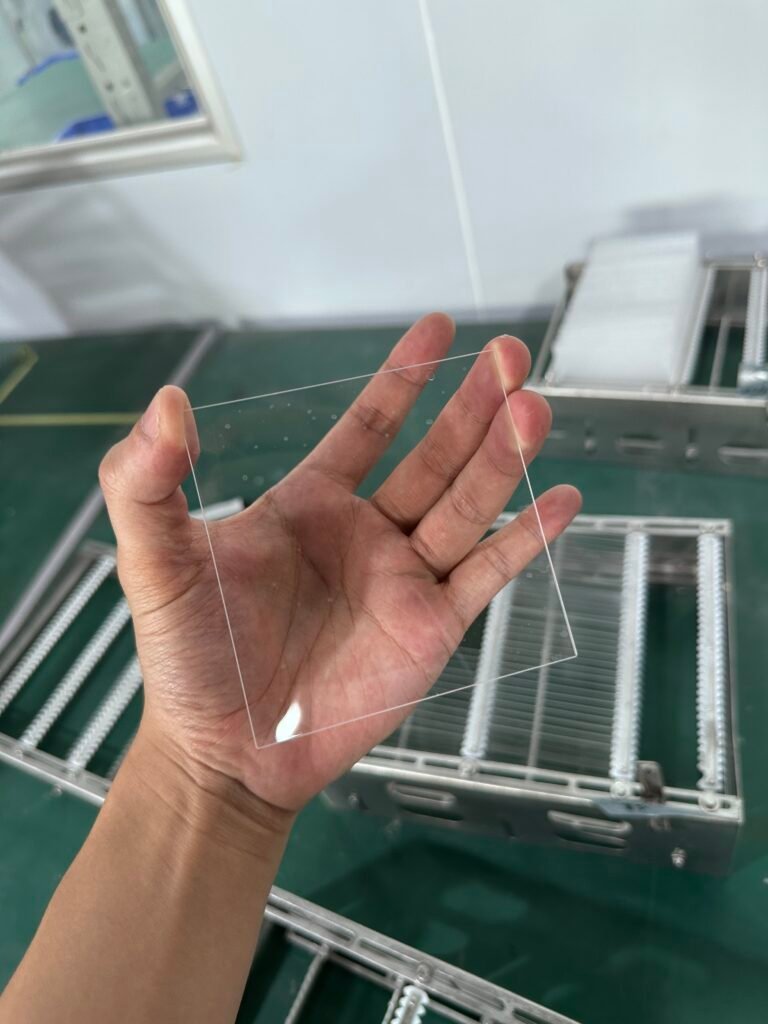
Double-sided polished glass has two faces finished for specified optical, dimensional or downstream-process requirements. It is used in windows, optical substrates, precision covers and glass wafers, but “double polished” is not a complete acceptance specification. A part can have smooth surfaces and poor thickness uniformity, or acceptable thickness variation and excessive bow. The drawing must distinguish these properties and define how each will be measured.
Polishing follows a controlled removal sequence
Grinding removes material and can establish shape or thickness while leaving damage and a comparatively rough texture. Lapping is controlled abrasive removal against a lap, commonly used to improve geometry or prepare for polishing. Polishing uses a finer finishing mechanism, often including chemical and mechanical interactions, to obtain the required surface condition. Neither a matte ground finish nor a reflective-looking surface alone establishes final optical quality.
Glass Double Side Polishing may use simultaneous processing of both faces, with the workpiece held in a carrier between working surfaces. Some parts are instead polished sequentially on opposite faces. The achievable geometry depends on material, thickness, carrier design, loading, removal allowance and process control. The phrase “double-sided polished” identifies the final faces; it does not prove that a particular simultaneous process or tolerance was used.
Separate the geometry quantities
| Quantity | Meaning | Acceptance details to state |
|---|---|---|
| Nominal thickness and tolerance | The allowed thickness level, distinct from within-part variation. | Where thickness is measured and whether local or average values govern. |
| TTV | Maximum minus minimum measured thickness within a defined area. | Mapping grid, edge exclusion, support, resolution and uncertainty. |
| Surface flatness | Departure of a specified surface from the stated reference-plane evaluation. | Clear aperture, support, reference construction, units and filtering. |
| Parallelism or wedge | Relative orientation of the two faces under an agreed evaluation. | Datum face, fitted planes, angular or linear expression and area. |
| Bow | A center-related deformation of the median surface relative to an agreed reference. | Free or constrained condition and reference-plane definition. |
| Warp | A range of median-surface departures from the defined reference plane. | Support, evaluated area and the particular definition used. |
TTV = tmax − tmin is a useful compact definition, but it is incomplete without the map area and measurement conditions. A uniformly thick curved plate can have low TTV and appreciable bow. A wedge-shaped plate can have locally smooth faces yet exhibit thickness variation. Flatness of one face, relative face orientation and median-surface shape therefore cannot be substituted for one another.
Optical surface figure and transmitted wavefront error also differ. Transmission through glass depends on both faces, thickness and refractive-index effects. When a requirement uses waves, specify the test wavelength and whether the reported quantity is surface departure or wavefront error. Avoid converting an interferometer result into a dimensional flatness limit without accounting for the actual test configuration.
Ra and Rq describe texture, not the entire surface
Ra characterizes average absolute profile height deviation; Rq uses a root-mean-square formulation and weights larger deviations differently. Results depend on the spatial bandwidth, filtering, evaluation length, instrument response and sampled location. An apparently impressive roughness value is not comparable to another result if these conditions differ. Areal Sa and Sq use an area rather than a line profile and should not be reported as Ra and Rq without explanation.
A contact profilometer, interferometric surface instrument and AFM can sample different spatial scales and have different artifacts. Transparent glass may produce reflections from both interfaces in an optical measurement; the selected surface must be identified. State the method, objective or sampling conditions, filtering and measurement sites. ISO 21920-2:2021 and ISO 25178-2:2021 provide the respective profile and areal parameter frameworks; ISO 10110-8:2019 addresses optical texture indications.
Scratch-dig is not a roughness specification
Scratch-dig addresses localized visible imperfections under a particular inspection convention. Ra describes sampled height statistics. A surface can satisfy one criterion and fail the other. The familiar 20/10 and 40/20 designations must identify the governing standard or agreed inspection method. In the traditional U.S. visibility convention, the scratch number is a comparison grade, not a direct scratch-width measurement; the dig designation relates to size under that convention.
ISO 10110-7:2017 provides ways to indicate permitted optical surface imperfections, including relevant test regions. Its notation should not be casually equated with a scratch-dig label. Define the clear aperture, defect inspection conditions, coating state and edge exclusions. Tighter defect grades should follow system sensitivity rather than being copied from another application. No universal 20/10 or sub-nanometer capability is established by this guide.
Applications place different priorities on the glass
In optical communication assemblies, FA/FAU-related covers may act primarily as structural or adhesive interfaces, whereas an optical window lies directly in the light path. Their relevant surface and geometry limits can differ substantially. A filter substrate adds coating requirements and sensitivity to surface figure or contamination. State the actual role instead of treating all telecommunications glass as one specification.
In MEMS or wafer-level packaging, thickness uniformity may affect processing and alignment, while bonding also depends on chemistry, particles and microscopic contact conditions. For TGV substrates, a polished incoming surface does not establish hole quality, metallization continuity or post-process geometry. Glass Wafer Polishing must be coordinated with drilling, cleaning, coatings and subsequent thermal cycles.
Glass wafers are not ordinary polished sheets
A wafer may need a defined diameter, edge contour, notch or orientation feature, handling compatibility and a map-based geometry requirement. A small rectangular window may instead be accepted over a clear aperture with edge mounting. Thin wafers are particularly sensitive to support, gravity and chucking during measurement. A clamped result can differ from free-state shape without either instrument being defective.
SEMI MF1530-0707, reapproved 0824, is a silicon-wafer metrology method and must not be presented as a universal glass-wafer specification. If a method is adapted to transparent glass, validate its sensing principle and conditions. SEMI 3D2 has a specific glass-carrier application scope; its cited 0216 reapproval 0222 listing is marked superseded. Confirm the applicable document and current purchasing requirements rather than assigning all glass wafers a silicon or carrier standard.
Material response affects the polishing route
Borosilicate glasses, aluminosilicate glasses, fused silica and optical glasses differ in composition and interaction with slurry chemistry. Removal rate, surface alteration, damage removal and cleaning behavior require material-specific evaluation. A sequence qualified for one glass should not be assumed suitable for another, even when both are sold as Optical Glass Substrates.
Size, thickness and aspect ratio are equally important. Carrier contact, pressure distribution and handling can affect edge roll-off or local removal. A thin, wide plate can be harder to inspect and handle than a thicker small window. Specifying “same finish as the sample” without retaining its material and geometry conditions is insufficient for repeatable Custom Glass Fabrication.
Match each requirement to an inspection method
Thickness mapping requires a calibrated method compatible with the material and thickness range. Record the map grid and edge exclusion rather than accepting only a single center reading. Surface-flatness inspection may use interferometry or another validated method; specify support, aperture, reference and treatment of tilt or other fitted terms. Parallelism needs its own two-face evaluation.
Texture inspection should report the instrument conditions and measured surface, while defect inspection should use the agreed lighting and comparison or dimensional method. Record uncertainty and how borderline results are decided. A measurement plan is especially important for transparent, thin or flexible glass because multiple reflections, mounting forces and support can affect the result.
Common defects and the final clean condition
Possible problems include residual grinding damage, pits, scratches, edge roll-off, uneven removal and particles introduced during handling. Their causes need investigation rather than inference from one photograph. For example, a scratch can arise during polishing, cleaning or packing; reworking the polishing step alone may not solve the problem. Inspect samples after the complete finishing and cleaning sequence.
Define acceptable cleaning residues, particles and packaging in relation to downstream use. Coating, optical contacting, adhesive bonding and semiconductor processing have different sensitivities. A visually clean surface is not proof of a specified contamination level. Packaging should protect both functional faces and allow unpacking without dragging them across abrasive or shedding materials.
Choose limits from the function and verify feasibility
An imaging window may prioritize surface figure, defects and spectral transmission; a bonding substrate may prioritize contact-compatible texture, contamination and global geometry; a structural cover may prioritize dimensions and assembly flatness. Glass TTV and Surface Roughness limits should be specified independently, at levels justified by the application. Prototype data should establish feasible capability for the actual material and dimensions before a production guarantee is agreed.
For a broader finish comparison, see ground versus polished glass selection. The geometry comparison guide provides a shorter introduction, while semiconductor substrate selection connects material choice with downstream processing.
Preparing a double-sided polished glass RFQ
Provide material grade, drawing revision, dimensions, nominal thickness, quantity and the intended functional faces. Specify applicable TTV, flatness, parallelism, bow or warp separately, including support and measurement conditions. Add profile or areal texture requirements, defect standard, clear aperture, edge contour, cleaning, coatings, packaging and downstream thermal or bonding processes. Request an agreed inspection plan and sample qualification rather than an unspecified “optical-grade” promise.
Review precision glass polishing · Review inspection requirements
Technical references
- ISO 10110-7:2017 — optical surface imperfections.
- ISO 10110-8:2019 — optical surface texture.
- ISO 21920-2:2021 — profile texture; ISO 25178-2:2021 — areal texture.
- SEMI MF1530-0707, reapproved 0824 — silicon-wafer method and scope.
- SEMI 3D2 — glass-carrier specification; listed reapproval 0222 is superseded.
- Edmund Optics — optical window surface-quality interpretation.
This article describes specification and verification logic, not verified company equipment or universal production capability. Contract requirements must be confirmed for the particular material, geometry and inspection plan.