LIGHTINGOptical Glass · Precision Processing
Contact UsChinese / English⌕
Semiconductor industry case study
CASE STUDY · Semiconductor and Microelectronics Glass

Semiconductor Industry Processing Case Study

For carriers, lids, wafers and micro-hole glass in semiconductor, MEMS and microelectronics projects, we plan material, precision processing and clean delivery as one workflow.
Project Overview

The complete route from material confirmation to finished-part delivery

Semiconductor-related glass parts often focus on thermal expansion, thickness uniformity, micro-holes or hole arrays, two-sided condition and cleanliness. Material selection must match downstream processes such as lithography, bonding, coating, packaging or inspection.

Typical components
Glass wafers, carriers, lids, micro-hole arrays, packaging windows
Main operations
Precision cutting, drilling, lapping and polishing, cleaning, inspection
Control focus
CTE, TTV, hole positions, surface, particles and traceability
Applications
MEMS, sensors, microelectronics and semiconductor equipment
Discuss a Similar Project
ENGINEERING GUIDE

Confirm the process first, then the glass

A glass wafer of the same size has different requirements as a carrier, an anodic bonding lid, a lithography substrate, a micro-hole interposer or an equipment window. Material name, process temperature, geometric specification, surface and packaging must be confirmed together.

Applications

Where it can be used

  • Glass lids and anodic bonding wafers for MEMS and sensors
  • Semiconductor process carriers, temporary carriers and thin-plate supports
  • Wafer-level packaging windows, spacers and transparent caps
  • Micro-hole/hole-array glass and via substrates for customer metallization
  • Viewing windows, insulating plates and optical components in semiconductor equipment
Material Selection Logic

Why glass

Glass combines transparency, electrical insulation, chemical stability and adjustable thermal expansion. Low-alkali glass reduces the risk of alkali metal migration; borosilicate glass suits glass-silicon thermal matching and anodic bonding; fused silica suits low-CTE, high-temperature, high-purity and specific spectral environments.

Material Selection

Common materials and their applications

MaterialApplicationsSelection focus
PYREX® Micro-ElectroMEMS, anodic bonding and wafer-level packagingCTE 3.43 × 10⁻⁶/°C(0–300°C)
BOROFLOAT® 33General wafers, sensing, microfluidics and equipment windowsCTE 3.25 × 10⁻⁶ K⁻¹, heat and chemical resistant
EAGLE XG® / alkali-free glassSubstrates for TFT, thin films, microelectronics and low-ion applicationsWatch the alkali content, strain point and pristine surface
Fused SilicaHigh-temperature, high-purity, low-CTE, UV/laser and equipment componentsConfirm the hydroxyl, impurities and spectral grade
Typical Parameters

Common enquiry parameters

ItemCommon starting points or wordingEngineering notes
Wafer diameterCommonly 100, 150, 200, 300 mmCompatible with equipment, cassettes, chucks and layout
ThicknessCommonly 0.20-1.10 mm; carriers may also be thickerAffects stiffness, thermal mass and the equipment focal plane
TTVStandard discussion from ≤10-25 μm; high-precision bonding can be evaluated to ≤1-5 μmDetermines the bonding gap, focal plane and local stress
Bow/WarpDefined individually by equipment and processState the measurement method and edge exclusion
Surface roughnessBonding/thin-film faces usually require nm-level controlValues must be given with the measurement bandwidth
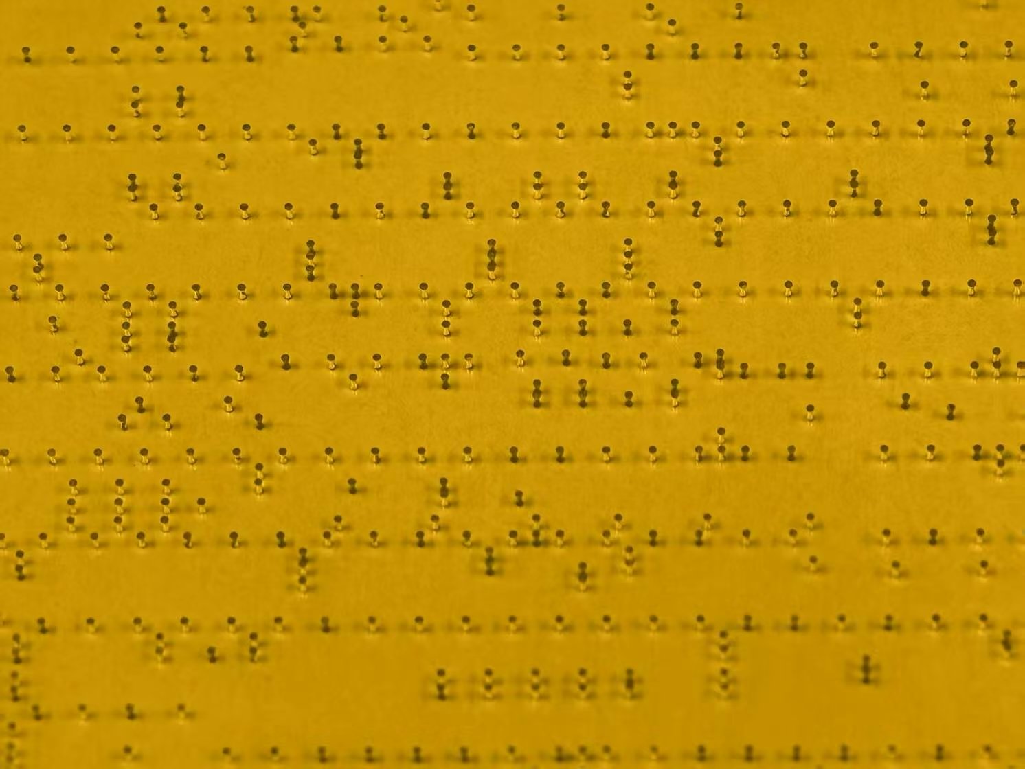
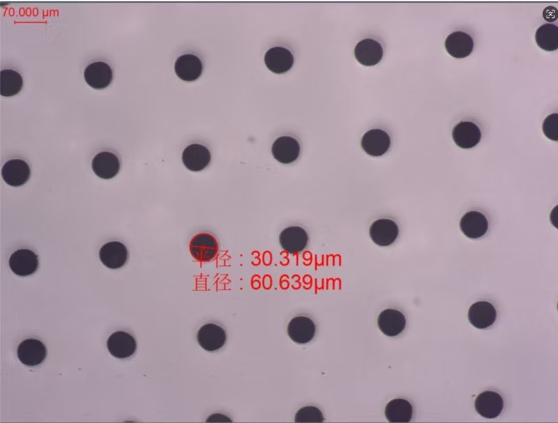
Micro-holesInlet/outlet hole diameter, taper, pitch, position tolerance and hole-to-edge distanceHole walls and the heat-affected zone affect downstream metallization and sealing
CleanlinessParticles, ions, metals and organic residueCommit only to grades for which inspection and control capability actually exists
Structure and Function

What it usually needs to look like

Available as standard wafers, square or rectangular carriers, discs with Flat/Notch, glass lid wafers, micro-hole arrays, package plates with windows/cavities, thin Spacers and equipment viewing windows.

  • Provide a stable carrier for lithography, thin films, bonding and packaging
  • As transparent lids, electrically insulating layers and dielectric structures
  • Carry micro-hole arrays and the customer's subsequent interconnect structures
  • Provide equipment-compatible dimensions, edges and locating references
Performance Requirements

Performance items recommended for confirmation

  • Material thermal expansion, strain point, alkali content and dielectric matching
  • Low TTV, controlled Bow/Warp and stable thickness
  • Low roughness, low particles and low residue on the functional face
  • Micro-hole position, taper, hole walls and heat-affected zone are controlled
  • Material lot, process lot, inspection and packaging traceability
Preparing Your Enquiry

Please provide in the drawing or enquiry

Process application, maximum temperature and atmosphere, silicon/film/adhesive materials, size and thickness, TTV, Bow/Warp, surface and roughness, micro-hole drawing, edge exclusion, particle/ion/metal limits, inspection method, quantity, lot and packaging. Where only glass micro-holes are supplied, it is not promoted as a complete TGV solution including metallization and reliability validation.

The parameters above are for preliminary material and process selection and do not constitute a uniform guarantee for all dimensions, thicknesses and materials. Final specifications, measurement methods and delivery standards are governed by the drawing, samples and order documents confirmed by both parties.

01

Downstream process confirmation

Understand the bonding, lithography, coating, packaging or equipment assembly conditions first, and define the material and cleanliness boundaries.

Semiconductor industry processing and material preparationSemiconductor industry processing inspection
02

Material and geometry planning

Select the material and process route from thermal expansion, thickness, dimensions, hole geometry and surface requirements.

03

Precision processing and in-process protection

Complete cutting, hole arrays, edge or double-sided processing, controlling particles and scratches during handling.

04

Inspection and clean delivery

Check dimensions, hole positions, edges and surface condition, and complete cleaning, separated packaging and batch delivery.

Start material selection and processing requirements from the same drawing

Send the drawing and key acceptance items and we will assess the project together with the material and process route.