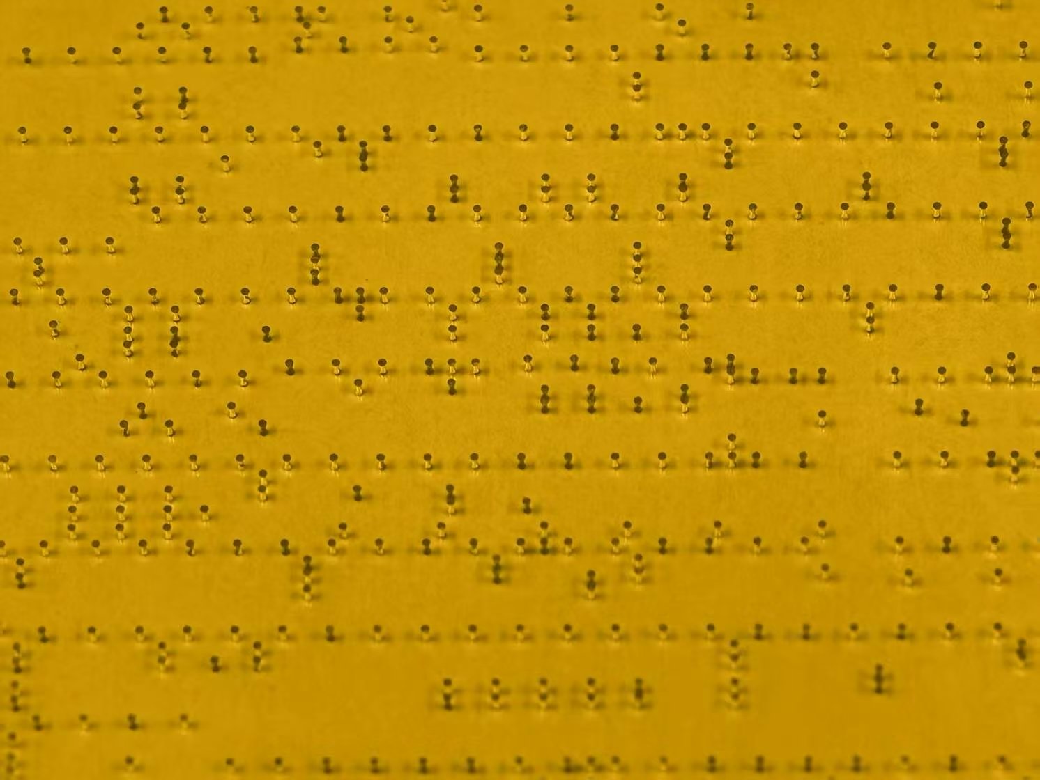
Semiconductor Industry Processing Case Study
For carriers, lids, wafers and micro-hole glass in semiconductor, MEMS and microelectronics projects, we plan material, precision processing and clean delivery as one workflow.
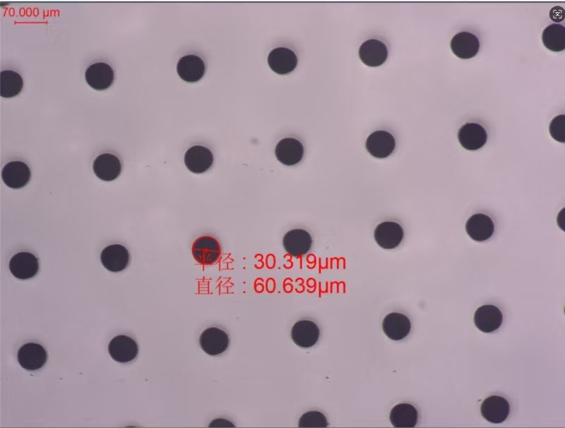
For carriers, lids, wafers and micro-hole glass in semiconductor, MEMS and microelectronics projects, we plan material, precision processing and clean delivery as one workflow.


Semiconductor-related glass parts often focus on thermal expansion, thickness uniformity, micro-holes or hole arrays, two-sided condition and cleanliness. Material selection must match downstream processes such as lithography, bonding, coating, packaging or inspection.
Understand the bonding, lithography, coating, packaging or equipment assembly conditions first, and define the material and cleanliness boundaries.


Select the material and process route from thermal expansion, thickness, dimensions, hole geometry and surface requirements.
Complete cutting, hole arrays, edge or double-sided processing, controlling particles and scratches during handling.
Check dimensions, hole positions, edges and surface condition, and complete cleaning, separated packaging and batch delivery.
Send the drawing and key acceptance items and we will assess the project together with the material and process route.