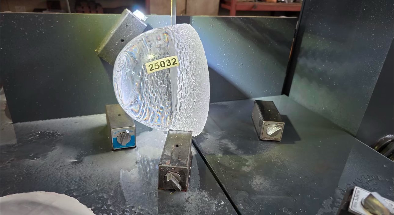
CASE STUDY · Wafer-Level Glass Processing
Glass Wafer Processing Case Study
For glass discs and wafer substrates, we control material, diameter, thickness, edges, two-sided condition, cleaning and packaging together.
For glass discs and wafer substrates, we control material, diameter, thickness, edges, two-sided condition, cleaning and packaging together.
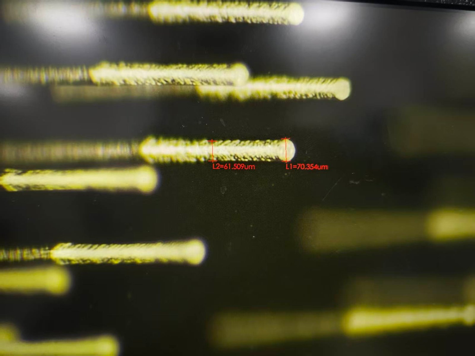
Glass wafers usually serve sensing, microelectronics, optics and packaging projects. Beyond diameter and thickness, attention should go to flatness, thickness variation, edge profile, two-sided appearance, orientation marking and clean packaging, with acceptance defined together with downstream coating, bonding or lithography processes.
Confirm material, diameter, thickness, flat or notch, effective area and downstream processes.
Establish the circular outline and edge structure, reducing edge chipping and later handling risk.
Lapping or double-sided polishing is carried out according to thickness, parallelism and surface requirements.
Check dimensions, edges, two-sided appearance and cleanliness, and package according to handling and downstream process requirements.
Send the drawing and key acceptance items and we will assess the project together with the material and process route.