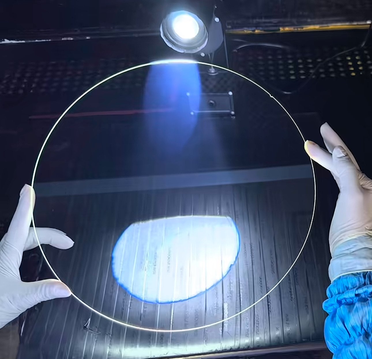
Formed with Corning's fusion draw process, it combines ultra-low alkali content, an excellent pristine surface, low thermal expansion and high dimensional stability, suited to wafer-level optics, display and microelectronic substrates.
EAGLE XG® is an alkali-free alkaline earth boro-aluminosilicate glass that contains no heavy metals such as arsenic, antimony or barium. Its thermal expansion is close to that of silicon, and it offers a relatively high strain point, optical transparency, chemical durability and inherent dimensional stability, making it suitable for wafer-level optics, electronic devices and display substrate projects.
Fusion pristine surfaceDuring forming the surface does not contact the forming medium, making it suitable for substrate projects sensitive to cleanliness and flatness.Alkali-free and thermally stableLow alkali content, a relatively high strain point and low thermal expansion suit display, optical and microelectronic processes.Wafer and thin-sheet supplyWafers, rectangular sheets and scribed sheets are supported, with prototyping, small-batch and volume delivery.
EAGLE XG® Material Characteristics
Corning's proprietary fusion draw process lets the glass form a flat thin sheet in air with stable thickness control. For wafer-level optics and semiconductor processing, surface roughness, TTV, warpage, edge condition and clean packaging must be confirmed alongside the material grade.
The material's average coefficient of linear thermal expansion from 0–300 °C is 3.4 × 10⁻⁶/°C and its strain point is 669 °C; the high thermal stability benefits downstream high-temperature processes. EAGLE XG® has a total alkali content of about 0.1 wt%, with typical values below 0.05 wt%.
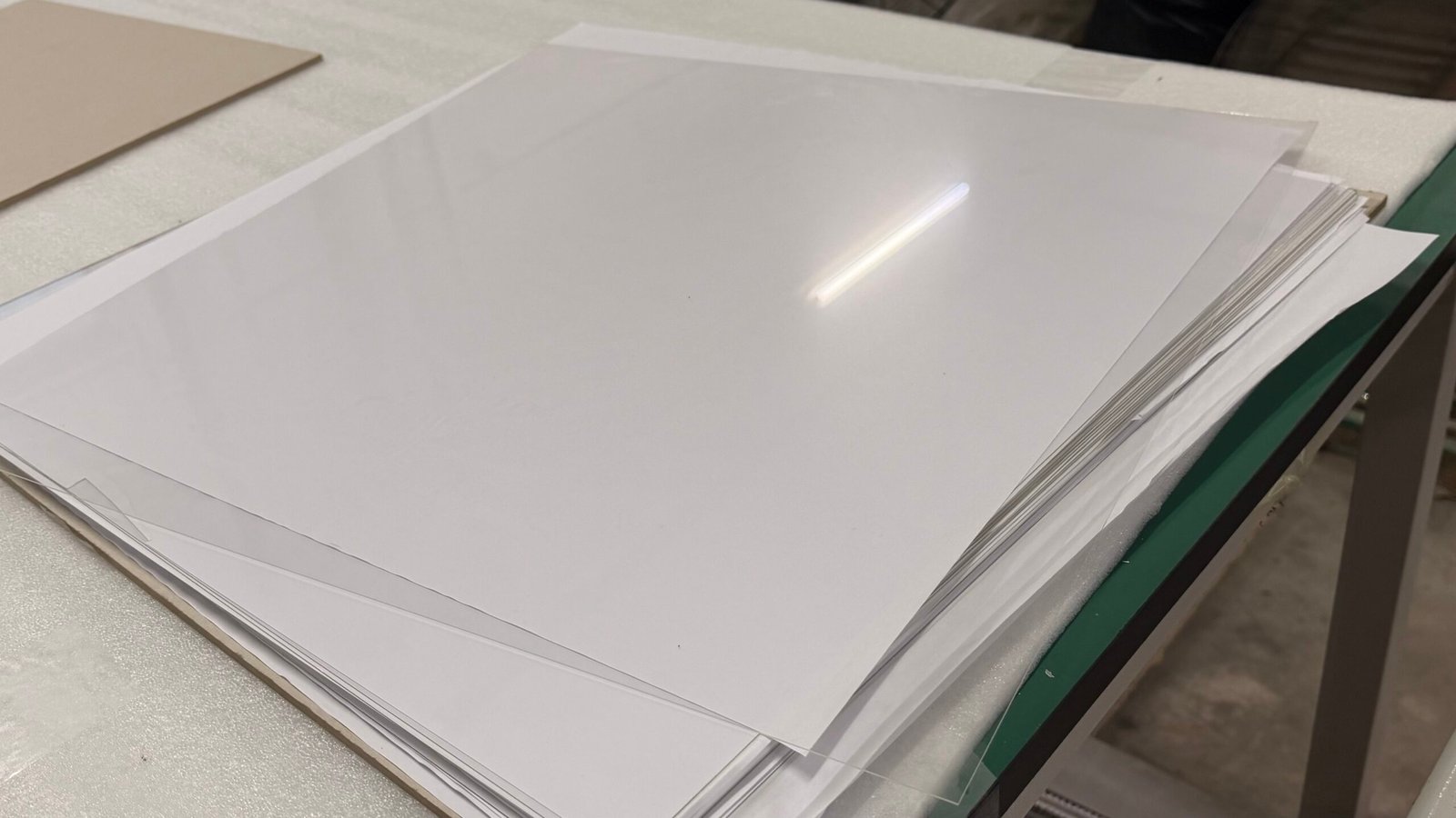
EAGLE XG® wafers, rectangular thin sheets and machined sample positions
Approximately 0.1 wt%; typical value below 0.05 wt%
The data above are typical or reference values from published documentation and are not guaranteed values for finished parts. Formal purchasing and acceptance are governed by the material documents for the corresponding batch, the drawing and specifications confirmed by both parties.
Supply Specifications
EAGLE XG® wafer and thin-sheet specifications
The following are the standard capabilities listed in the Corning Precision Glass Solutions data sheet; stock, minimum order quantity and lead time are confirmed per project.
Outline ±0.3 mm; thickness ±0.01 mm; scratch/dig 60/40 to 20/10; Ra ≤ 10 Å
Tighter dimensional, thickness, surface and edge requirements can be assessed against the drawing; formal acceptance is governed by the specification confirmed by both parties.
Material + Processing
From EAGLE XG® thin glass to assembly-ready precision substrates
Processing focuses on minimising surface contact and treating fixturing, edges, cleaning, inspection and packaging as one continuous flow.
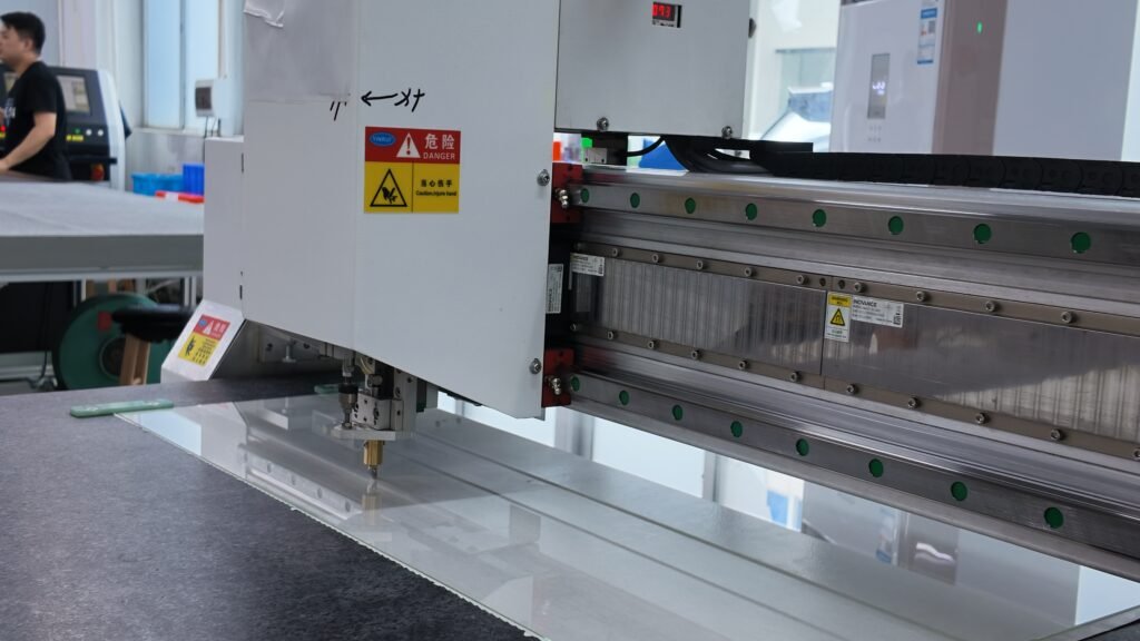
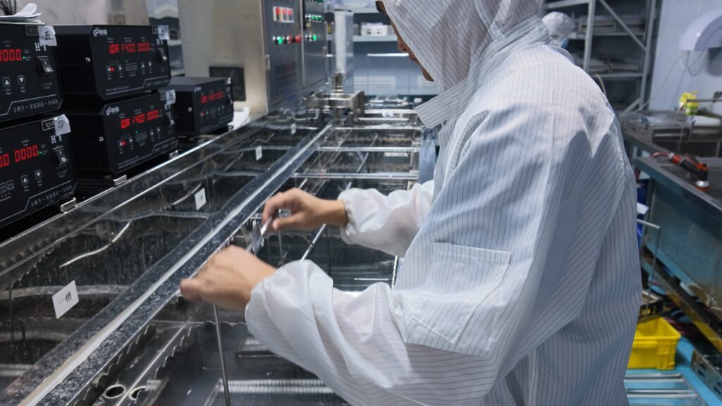
Precision cutting and dicingThe cutting path and fixturing are planned according to wafer or rectangular sheet size, thickness and permitted chipping.Edges, cleaning and protectionFor ultra-thin glass we control edge micro-chipping, particle residues, water marks, protective film and handling method.Dimensional and appearance inspectionDimensions, thickness, TTV, warpage, surface quality and clean packaging requirements are confirmed per project.
For enquiries, please provide outline, thickness, quantity, tolerances, edge style, surface grade, clean packaging, application and required lead time; include a drawing if available.
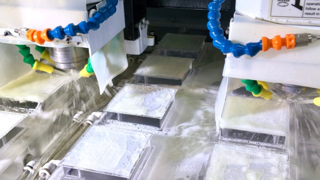
We plan the glass cutting route around dimensions, datums, edge condition and downstream operations, reviewing outline, cutting allowance and delivery requirements against the drawing.
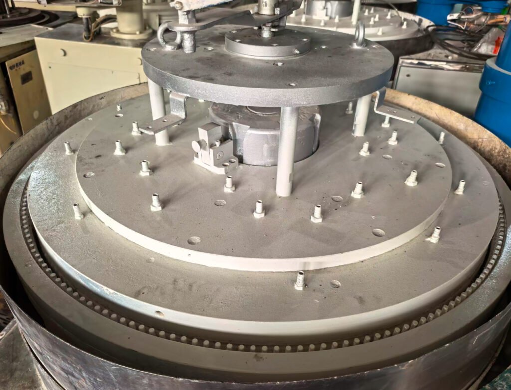
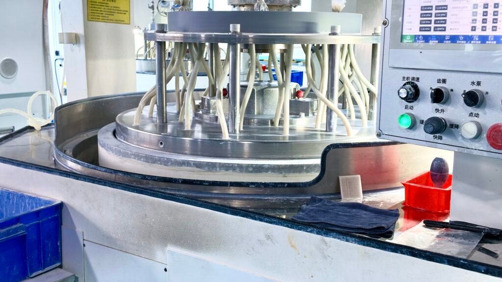
Grinding and polishing operations are arranged around thickness, parallelism, flatness and surface requirements, with the process route and inspection method confirmed per project.
We control particles, residues and water marks after processing, and confirm cleaning, handling and packaging requirements against coating, bonding or assembly needs.
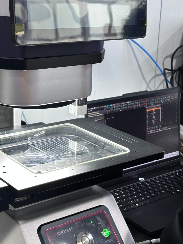
Glass dimensions, edges and surfaces are inspected against the drawing and the agreed acceptance items, with inspection methods, sampling scope and delivery records defined.
We address sharp edges and local edge defects after cutting, confirming edge grinding and chamfer styles and edge acceptance criteria against assembly requirements.
Material selection still needs to be confirmed against temperature, structure, thickness, surface and downstream processes together.
Wafer-level opticsMicro-optical arrays, wafer-level lenses and optical substrates needing a high-quality surface.Display and touchDisplay backplanes, touch and electronic glass R&D samples.Semiconductor and sensingCarriers, package lids, sensor substrates and microelectronic structures.R&D validationMaterial and process validation across multiple thicknesses, small batches and custom outlines.
Purchasing FAQ
Frequently asked questions about buying EAGLE XG®
What type of glass is EAGLE XG®?
It is an alkali-free alkaline earth boro-aluminosilicate glass produced with Corning's fusion draw process, intended for display, wafer-level optics and microelectronic substrate applications.
Which wafers and thicknesses are available?
The published data sheet lists 100, 150, 200 and 300 mm wafers and thicknesses of 0.20, 0.21, 0.25, 0.30, 0.40, 0.50 and 0.70 mm; actual stock and lead time are confirmed by enquiry.
Can you supply tighter dimensional specifications?
Tighter dimensional, thickness, surface and edge requirements can be discussed per project; final capability is subject to drawing assessment and the confirmed specification.
Why do thin glass projects need particular attention to edges?
Tiny edge chips can affect handling, assembly and service strength, so the cutting path, fixturing, edge treatment and protective packaging must be planned together.
What information is needed for an enquiry?
Please provide outline, thickness, quantity, tolerances, edges, surface, clean packaging, application and lead time; include a drawing if available.
Put the EAGLE XG® material specification and processing requirements in one enquiry
Provide the wafer or sheet size, thickness, quantity and key acceptance items, and we will match cutting, edge, cleaning and inspection processes to the material's characteristics.