LIGHTINGOptical Glass · Precision Processing
Contact Us中文 / English⌕
Corning PYREX
CORNING® PYREX® MICRO-ELECTRO

Corning® PYREX® Micro-Electro Glass

A borosilicate glass for wafer-level packaging and microelectronic processes

Combining thermal expansion close to silicon, optical transparency, dielectric performance and wafer-processing consistency, it suits MEMS, sensor and microfluidic projects.
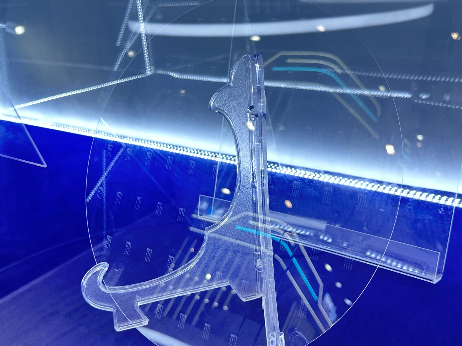
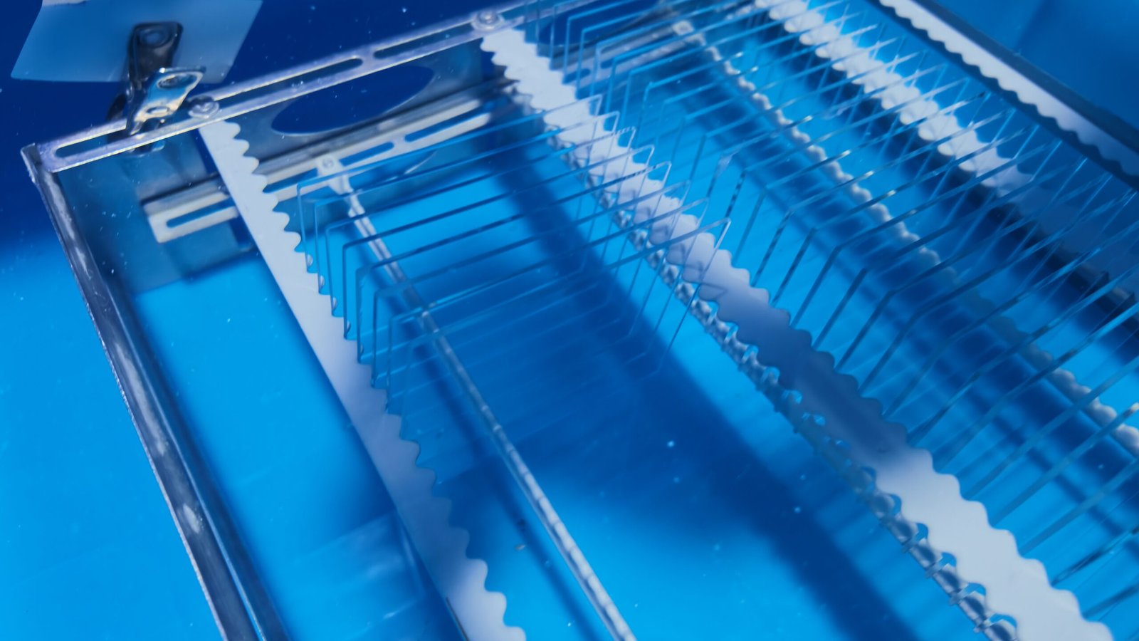
Material Positioning

A stable glass base for silicon devices, microstructures and optical windows

Material selection starts from thermal matching, surface quality, thickness consistency and the bonding process, and is then translated into inspectable drawing requirements.

01Silicon-matched thermal expansion

Typical CTE from 0–300 °C is 3.43 × 10⁻⁶/°C, suitable for evaluating anodic bonding and wafer-level packaging.

02Built for wafer processes

Delivery specifications can be built around wafer diameter, thickness, TTV, warpage and edge form.

03Both optical and electrical performance

With visible-light transparency and published dielectric parameters, it can be used in optical sensing and microelectronic structures.

Material Introduction

From sheet to glass wafers ready for downstream processes

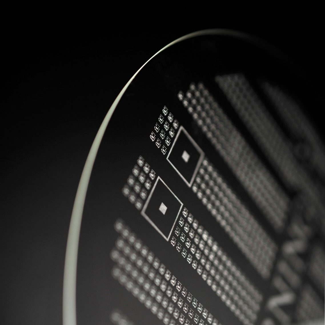
PYREX® Micro-Electro is a borosilicate glass intended for microelectronic and wafer-level applications, suited to projects needing glass–silicon thermal matching, optical windows, electrical insulation or package lids.

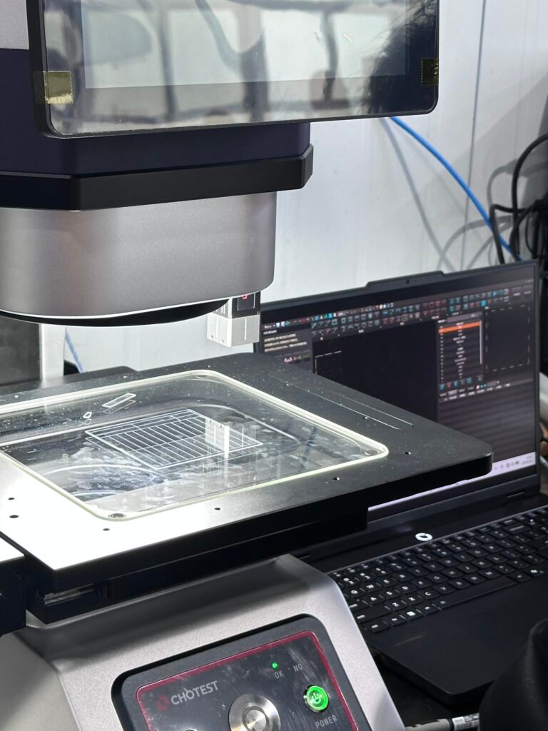
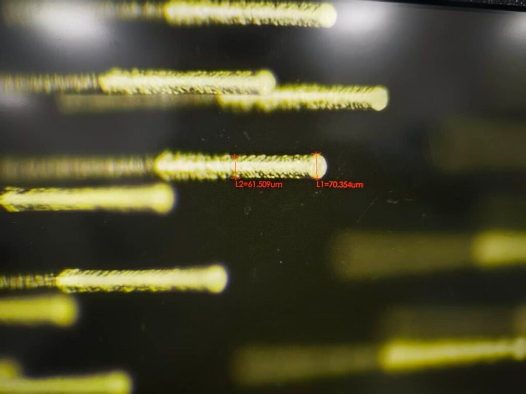
What usually affects delivery is not the material name itself but thickness, TTV, warpage, edge quality, surface cleanliness and packaging. We assess these against the drawing together with cutting, lapping, polishing, cleaning and inspection.

pyrex
Material Data Sheet

PYREX® Micro-Electro Basic Performance Parameters

Download the official PDF ↓
Density2.234 g/cm³
Young's modulus61.5 GPa
Poisson's ratio / shear modulus0.19 / 25.8 GPa
Vickers hardness520 kgf/mm² (200 g load)
Coefficient of thermal expansion (CTE)3.43 × 10⁻⁶/°C(0–300°C)
Softening point / annealing point / strain point814°C / 546°C / 498°C
Thermal conductivity1.10 W/(m·K)(50°C);1.56 W/(m·K)(500°C)
Refractive index1.472(589.3 nm)
Dielectric constant / loss tangent4.68 / 0.0041(0.5 GHz);4.55 / 0.0084(10 GHz)
Volume resistivitylog₁₀ ρ = 8.01 Ω·cm(250°C)
The above are typical or reference values from official Corning documentation and are not guaranteed values for finished parts. Formal purchasing and acceptance are governed by the material documents for the corresponding batch, the drawing and specifications confirmed by both parties.
Supply Specifications

PYREX® Micro-Electro wafer and panel specifications

Standard and custom capability must be confirmed against stock, batch, process route and project acceptance conditions.

Typical formsWafer / rectangular sheet / custom outline
Common thicknesses0.20–1.40 mm
Standard thickness

0.20 · 0.50 · 0.70 · 0.85 · 1.10 · 1.40 mm

Size range

Wafer specifications confirmed per project; panels can be assessed up to 600 × 600 mm

Geometric quality

TTV, warpage, thickness tolerances and surface requirements confirmed against the drawing and process together

Wafer TTV can be assessed to ≤1 μm; panel and wafer warpage capability depends on dimensions, thickness and measurement conditions; formal metrics must be written into the confirmed specification.

Material + Processing

From PYREX® wafers to bondable, packagable glass components

The process route is designed around low-damage edges, thickness consistency, surface cleanliness and downstream process compatibility.

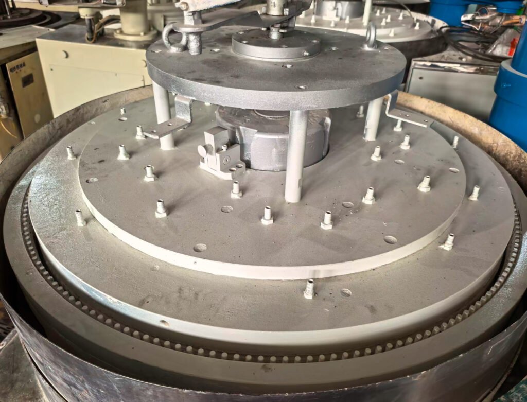
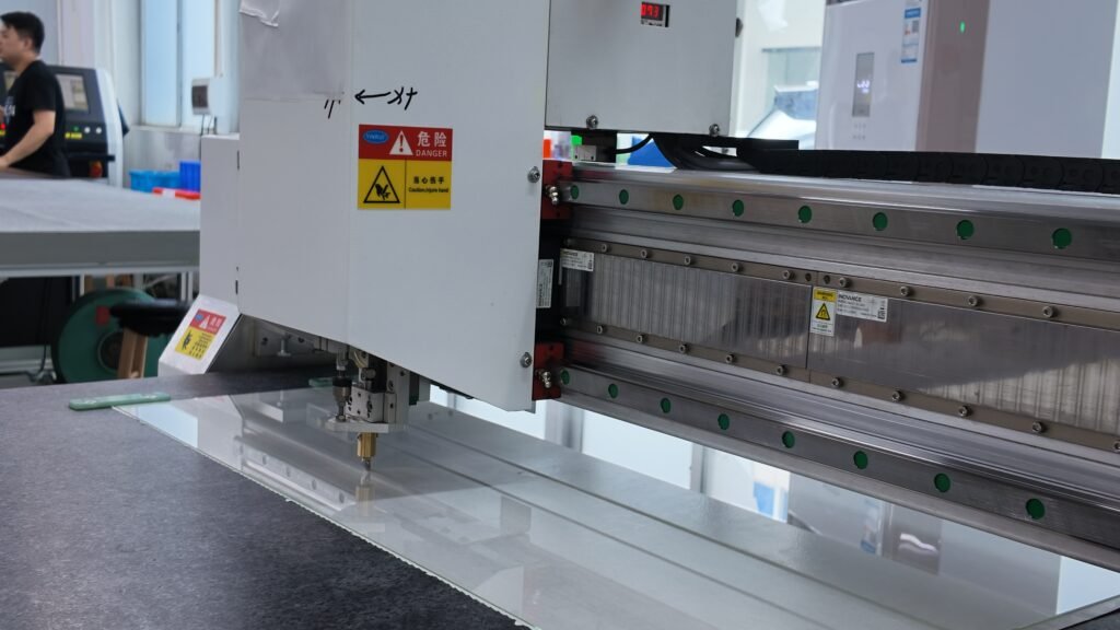
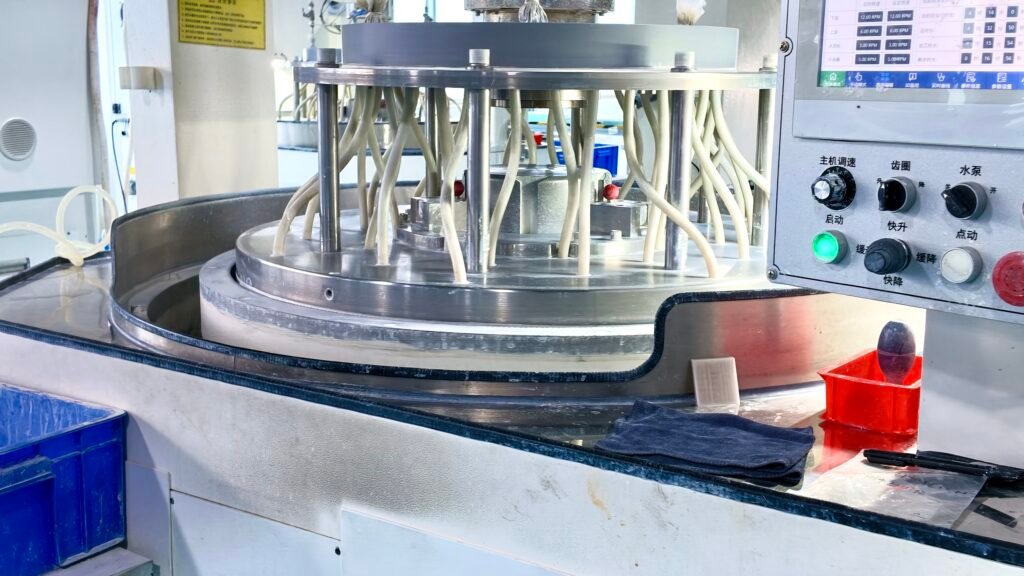
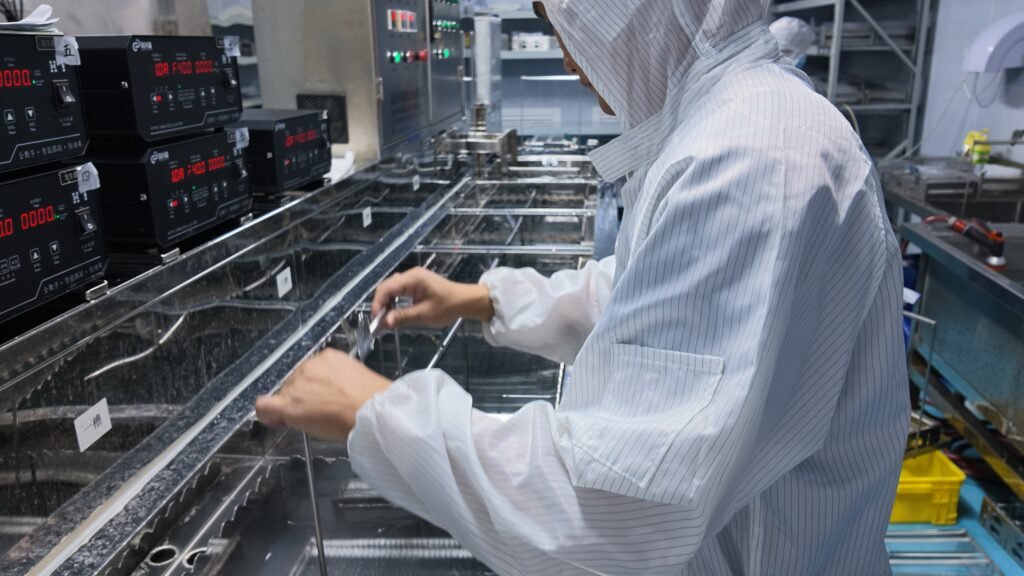
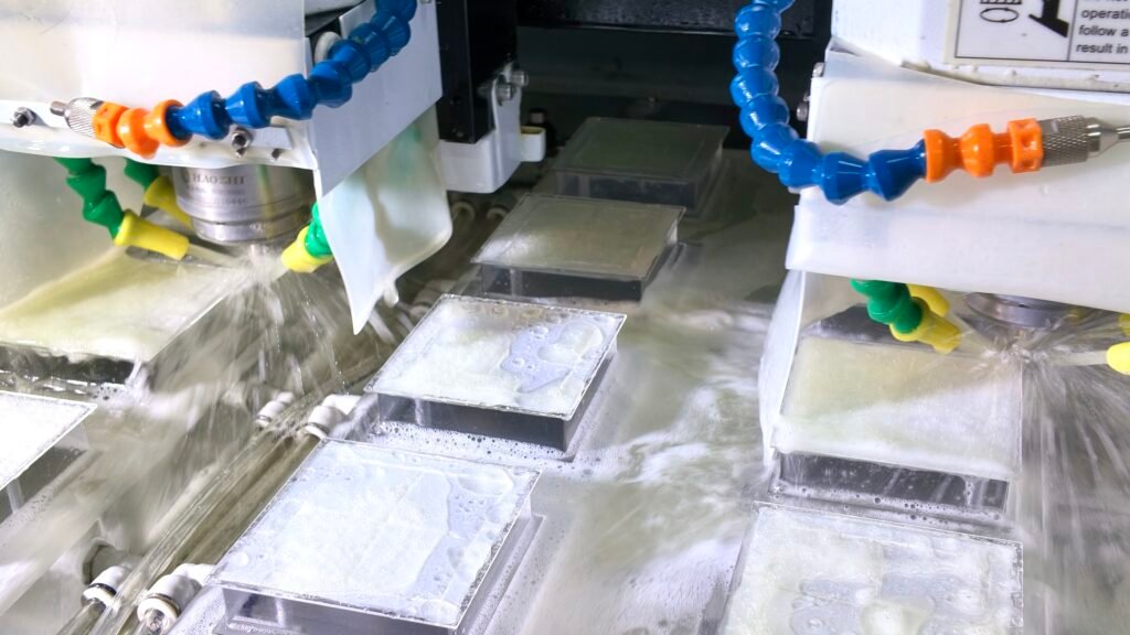
PYREX Micro-Electro glass precision processing
Wafer and profile cuttingCutting and fixturing are planned around outline, thickness and permitted chipping.
Lapping, polishing and TTV controlThe process is set by flatness, roughness and thickness consistency.
Cleaning, inspection and clean packagingThe delivery flow is built around bonding, packaging and optical use requirements.
For enquiries, please provide outline, thickness, quantity, tolerances, edge style, surface grade, clean packaging, application and required lead time; include a drawing if available.
Typical Applications

Projects Suited to PYREX® Micro-Electro

Suitability should be validated against temperature cycling, structural stress, bonding method, optical band and cleanliness requirements.

MEMS and sensorsPressure, inertial, microfluidic and other microstructured devices needing a glass lid.
Wafer-level packagingAnodic bonding, hermetic packaging and glass–silicon composite structures.
Optical windowsMiniature optics, imaging, inspection and transparent electrically insulating windows.
R&D and small-batch validationProcess validation projects with multiple sizes, thicknesses and custom outlines.
Purchasing FAQ

Frequently asked questions about buying PYREX® Micro-Electro

How does it differ from ordinary borosilicate glass?

This material is intended for microelectronic and wafer-level applications, and purchasing places more emphasis on inspectable metrics such as TTV, warpage, surface, edges and cleanliness.

Can it be used for anodic bonding?

Its thermal expansion makes it suitable for glass–silicon bonding evaluation, but voltage, temperature, surface and cleanliness still need to be validated for the specific equipment and structure.

Which thicknesses and sizes are available?

Published documentation lists a range of wafer and thin-sheet specifications; actual available sizes, quantities and lead times are confirmed by enquiry against the drawing.

Can you supply tighter TTV or warpage?

We can assess this, but capability depends on dimensions, thickness, processing allowance and measurement method and must be confirmed before ordering.

What information is needed for an enquiry?

Please provide outline, thickness, quantity, TTV, warpage, edges, surface, clean packaging, application and lead time.

State the PYREX® material specification and wafer processing requirements in one go

Send the drawing, quantity and key acceptance items, and we will confirm material, process route, inspection method and lead time accordingly.