ТЕХНИЧЕСКОЕ РУКОВОДСТВО
Confirm the process first, then the glass
A glass wafer of the same size has different requirements as a carrier, an anodic bonding lid, a lithography substrate, a micro-hole interposer or an equipment window. Material name, process temperature, geometric specification, surface and packaging must be confirmed together.
Applications
Where it can be used
- Glass lids and anodic bonding wafers for MEMS and sensors
- Semiconductor process carriers, temporary carriers and thin-plate supports
- Wafer-level packaging windows, spacers and transparent caps
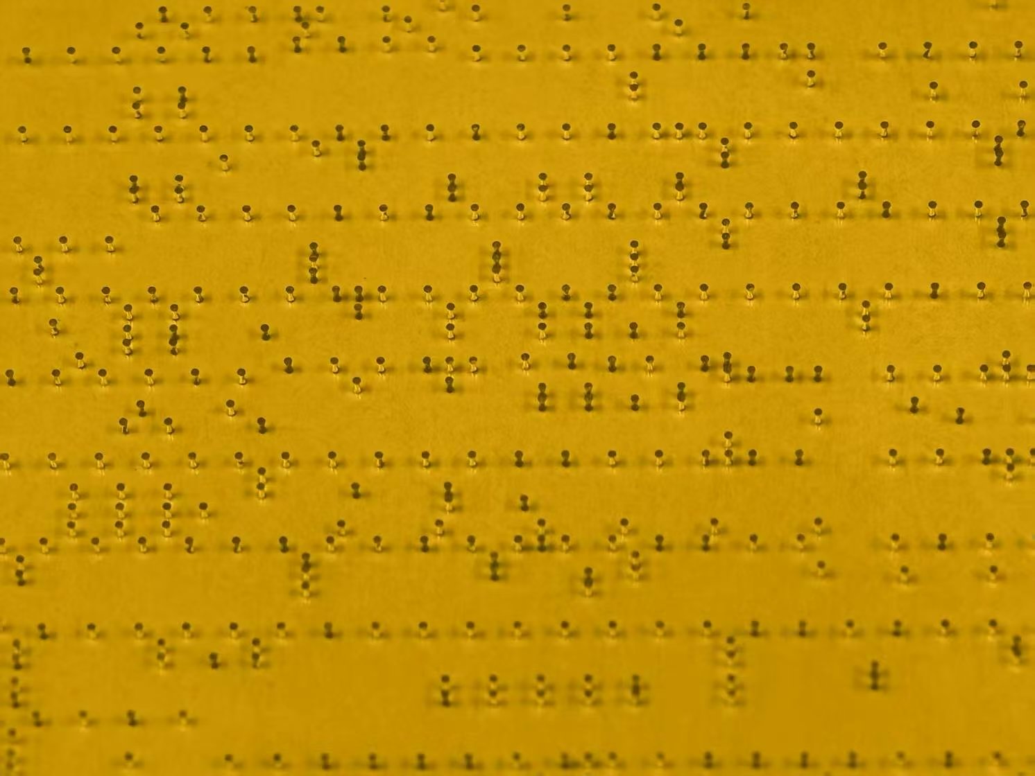
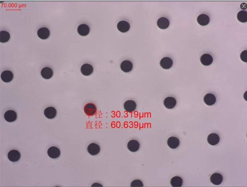
- Micro-hole/hole-array glass and via substrates for customer metallization
- Viewing windows, insulating plates and optical components in semiconductor equipment
Material Selection Logic
Why glass
Glass combines transparency, electrical insulation, chemical stability and adjustable thermal expansion. Low-alkali glass reduces the risk of alkali metal migration; borosilicate glass suits glass-silicon thermal matching and anodic bonding; fused silica suits low-CTE, high-temperature, high-purity and specific spectral environments.
Material Selection
Common materials and their applications
| Material | Applications | Selection focus |
|---|
| Borosilicate glass for qualified bonding | MEMS, anodic bonding and wafer-level packaging | Confirm grade-specific CTE and the qualified bonding recipe |
| BOROFLOAT® 33 | General wafers, sensing, microfluidics and equipment windows | CTE 3.25 × 10⁻⁶ K⁻¹, heat and chemical resistant |
| Alkali-free glass substrates | Substrates for TFT, thin films, microelectronics and low-ion applications | Confirm grade-specific ion content, thermal history and surface condition |
| Fused Silica | High-temperature, high-purity, low-CTE, UV/laser and equipment components | Confirm the hydroxyl, impurities and spectral grade |
Typical Parameters
Common enquiry parameters
| Item | Common starting points or wording | Engineering notes |
|---|
| Wafer diameter | Commonly 100, 150, 200, 300 mm | Compatible with equipment, cassettes, chucks and layout |
| Толщина | Commonly 0.20-1.10 mm; carriers may also be thicker | Affects stiffness, thermal mass and the equipment focal plane |
| TTV | Standard discussion from ≤10-25 μm; high-precision bonding can be evaluated to ≤1-5 μm | Determines the bonding gap, focal plane and local stress |
| Коробление / изгиб | Defined individually by equipment and process | State the measurement method and edge exclusion |
| Surface roughness | Bonding/thin-film faces usually require nm-level control | Values must be given with the measurement bandwidth |
| Micro-holes | Inlet/outlet hole diameter, taper, pitch, position tolerance and hole-to-edge distance | Hole walls and the heat-affected zone affect downstream metallization and sealing |
| Cleanliness | Particles, ions, metals and organic residue | Commit only to grades for which inspection and control capability actually exists |
Structure and Function
What it usually needs to look like
Available as standard wafers, square or rectangular carriers, discs with Flat/Notch, glass lid wafers, micro-hole arrays, package plates with windows/cavities, thin Spacers and equipment viewing windows.
- Provide a stable carrier for lithography, thin films, bonding and packaging
- As transparent lids, electrically insulating layers and dielectric structures
- Carry micro-hole arrays and the customer's subsequent interconnect structures
- Provide equipment-compatible dimensions, edges and locating references
Performance Requirements
Performance items recommended for confirmation
- Material thermal expansion, strain point, alkali content and dielectric matching
- Low TTV, controlled Bow/Warp and stable thickness
- Low roughness, low particles and low residue on the functional face
- Micro-hole position, taper, hole walls and heat-affected zone are controlled
- Material lot, process lot, inspection and packaging traceability
Preparing Your Enquiry
Please provide in the drawing or enquiry
Process application, maximum temperature and atmosphere, silicon/film/adhesive materials, size and thickness, TTV, Bow/Warp, surface and roughness, micro-hole drawing, edge exclusion, particle/ion/metal limits, inspection method, quantity, lot and packaging. Where only glass micro-holes are supplied, it is not promoted as a complete TGV solution including metallization and reliability validation.
The parameters above are for preliminary material and process selection and do not constitute a uniform guarantee for all dimensions, thicknesses and materials. Final specifications, measurement methods and delivery standards are governed by the drawing, samples and order documents confirmed by both parties.